Overlay measurements using zero-order cross polarization measurements

a cross-polarization measurement and overlay technology, applied in the field of overlay, can solve the problems of affecting the performance of devices/circuits, and conventional optical imaging systems typically have an accuracy of only about 5 to 10 nm

Inactive Publication Date: 2005-09-20
TOKYO ELECTRON US HOLDINGS INC
View PDF30 Cites 58 Cited by
  • Summary
  • Abstract
  • Description
  • Claims
  • Application Information

AI Technical Summary

Problems solved by technology

Misalignment of these masks, which is generally referred to as “overlay error”, can adversely affect the performance of the devices / circuits.
However, a conventional optical imaging system typically has an accuracy of only about 5 to 10 nm.

Method used


Image

  • Overlay measurements using zero-order cross polarization measurements
  • Overlay measurements using zero-order cross polarization measurements
  • Overlay measurements using zero-order cross polarization measurements

Examples


Embodiment Construction

[0027]The following description sets forth numerous specific configurations, parameters, and the like. It should be recognized, however, that such description is not intended as a limitation on the scope of the present invention, but is instead provided as a description of exemplary embodiments.

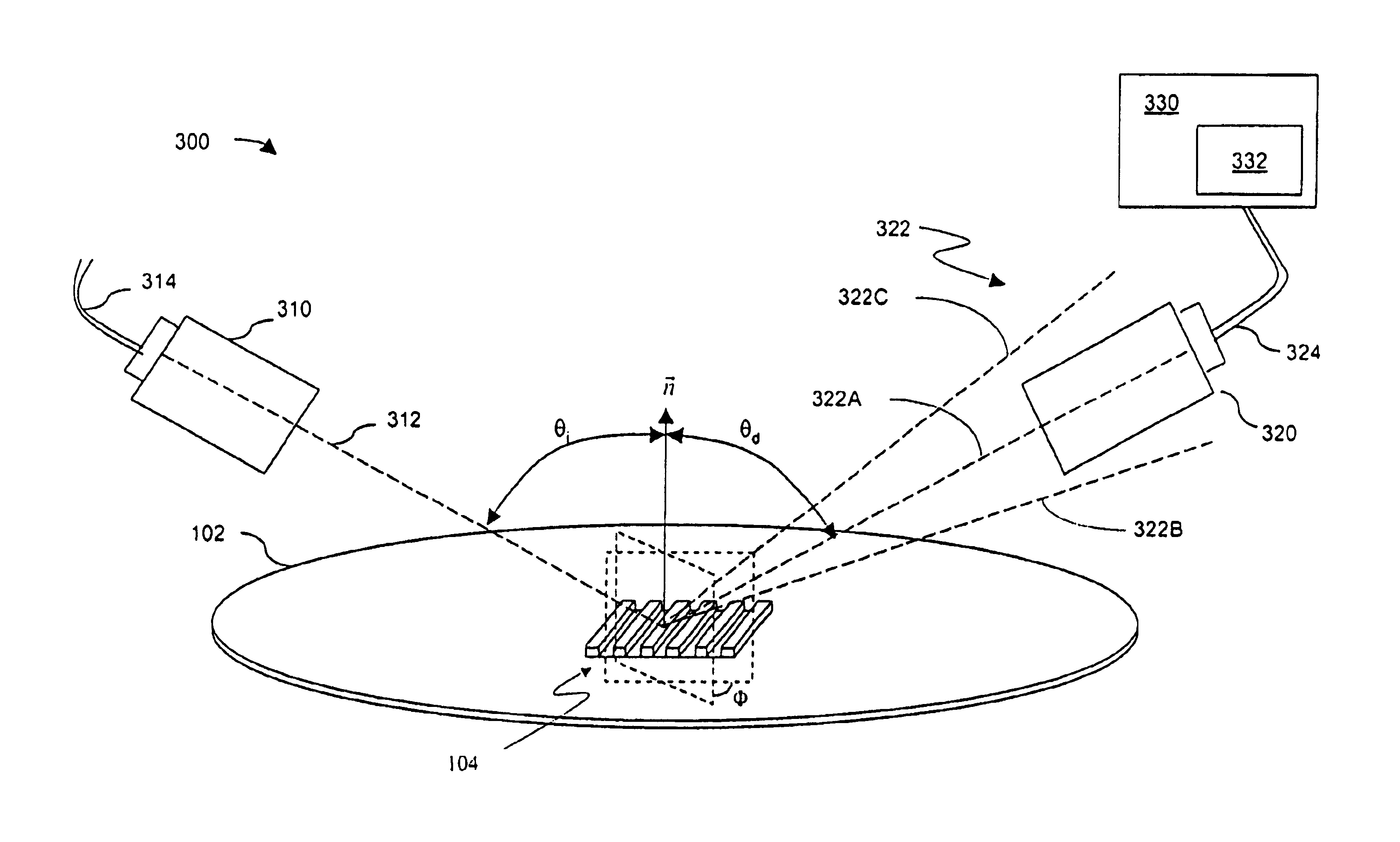
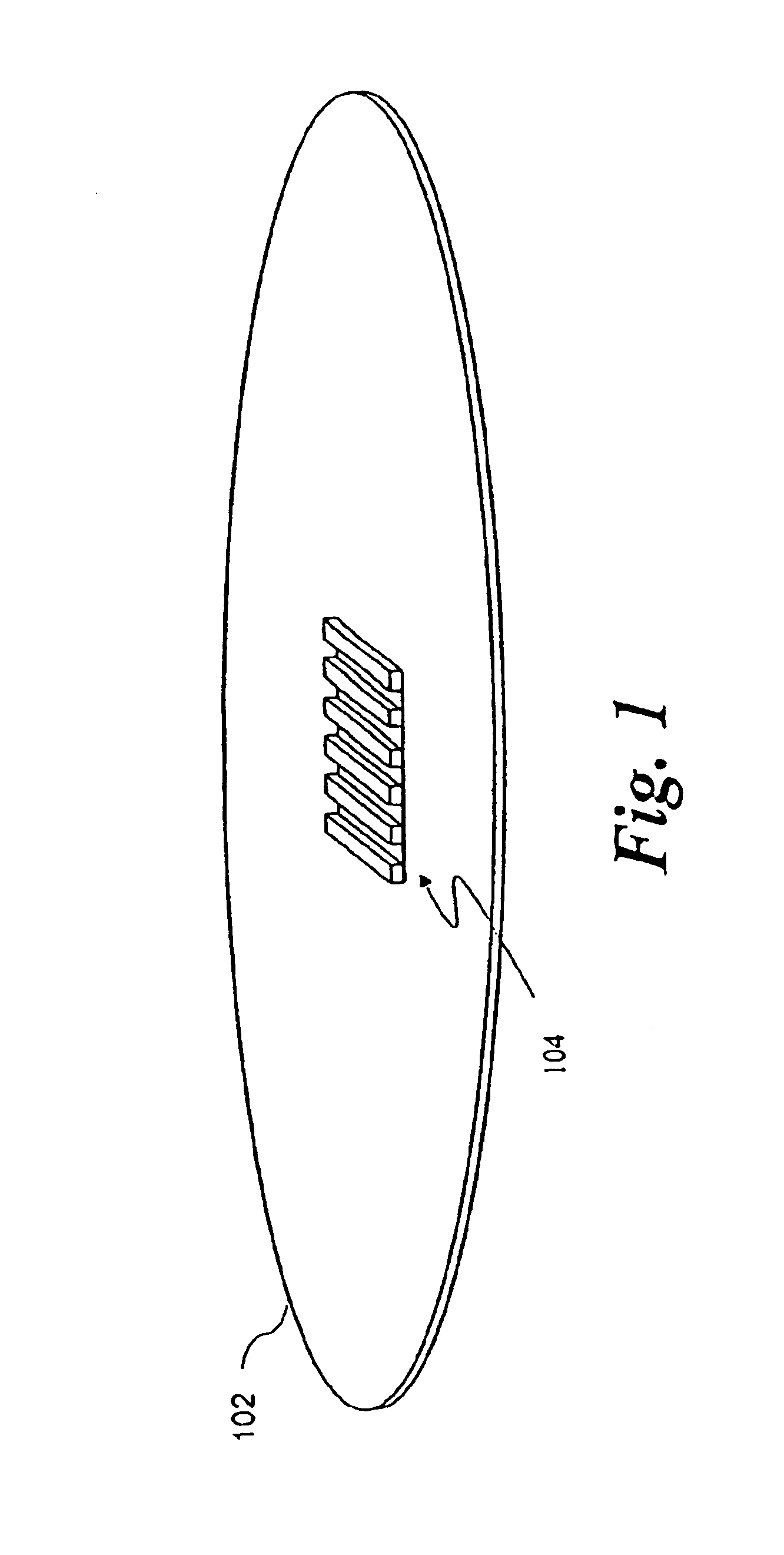
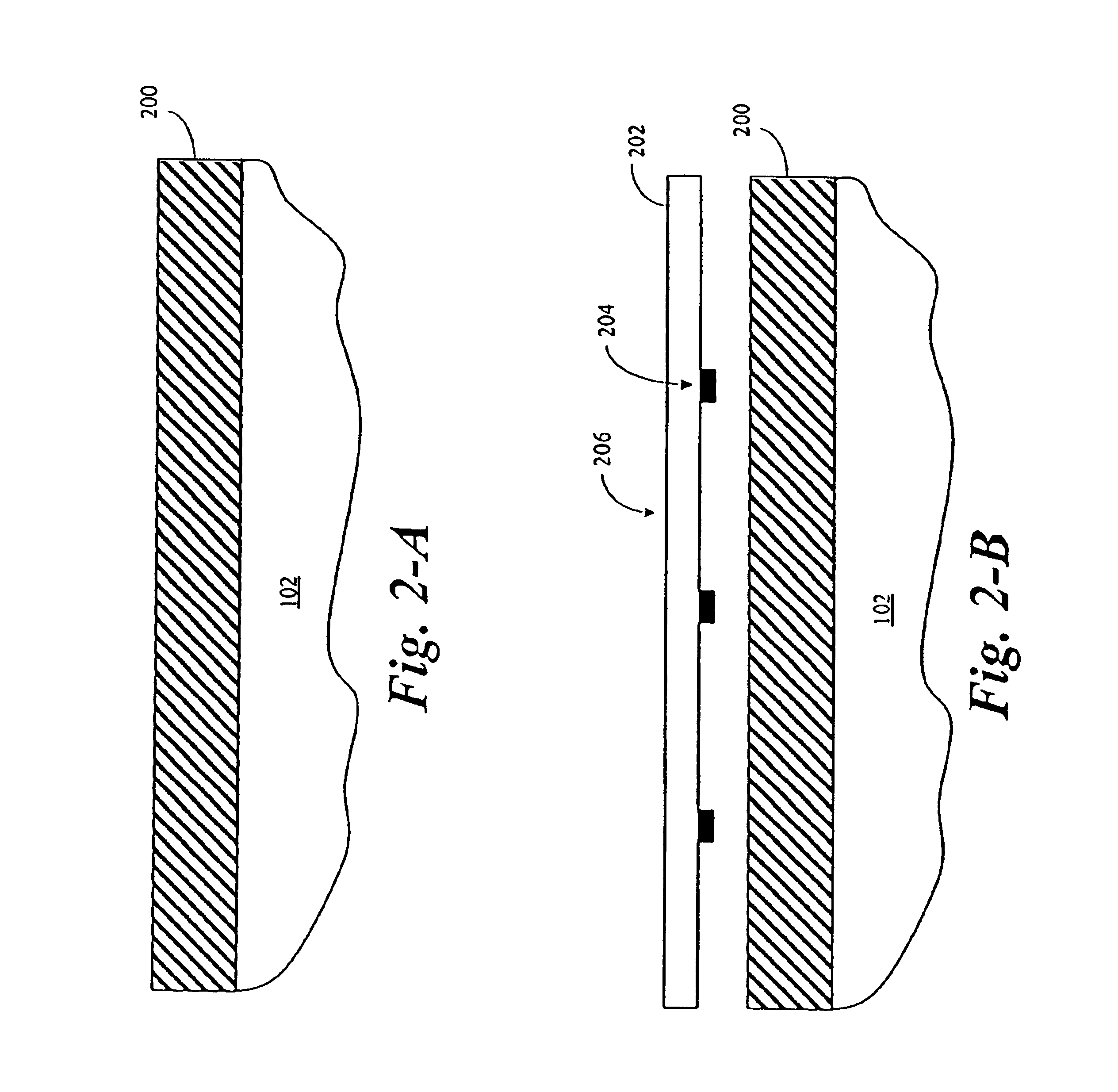
[0028]With reference to FIG. 1, as discussed earlier, the process of fabricating semiconductor devices / circuits on wafer 102 includes depositing and patterning layers of materials on wafer 102. More particularly, the features of the semiconductor devices / circuits are formed one layer at a time by depositing a layer of material, then removing portions of the deposited layer of material.

[0029]The process of depositing the layers of material is generally referred to as a disposition process. Exemplary deposition processes include chemical vapor deposition (CVD), oxidation, spin coating, sputtering, and the like. Exemplary materials that are deposited include oxides, metals, and the like.

[0030]Th...


PUM

PropertyMeasurementUnit
sizeaaaaaaaaaa
azimuthal angleaaaaaaaaaa

Abstract

Overlay measurements for a semiconductor wafer are obtained by forming a periodic grating on the wafer having a first set of ridges and a second set of ridges. The first and second sets of ridges are formed on the wafer using a first mask and a second mask, respectively. After forming the first and second sets of gratings, zero-order cross polarization measurements of a portion of the periodic grating are obtained. Any overlay error between the first and second masks used to form the first and second sets of gratings is determined based on the obtained zero-order cross polarization measurements.

Description

[0001]The present application is a continuation of U.S. patent application Ser. No. 10 / 138,903 filed May 2, 2002, now U.S. pat. No. 6,804,005 the entire content of which is incorporated herein by reference.BACKGROUND[0002]1. Field of the Invention[0003]The present invention relates to wafer metrology, and more particularly to obtaining overlay measurements for a semiconductor wafer using zero-order cross polarization measurements obtained from a periodic grating formed on the wafer.[0004]2. Related Art[0005]Semiconductor devices / circuits are formed on semiconductor wafers by depositing and patterning layers of materials. In general, the features of the devices / circuits are formed onto the layers of deposited materials using a patterning process.[0006]In a typical patterning process, the features of the devices / circuits are laid out, one layer at a time, on a series of photomasks (masks). The layout of the features of the devices / circuits on the masks are transferred, one mask at a t...

Claims


Application Information

Patent Timeline
Patent Type & Authority Patents(United States)
IPC IPC(8): G03F7/20
CPCG03F7/70633
Inventor BISCHOFF, JOERGNIU, XINHUI
Owner TOKYO ELECTRON US HOLDINGS INC
Why Eureka
Try Eureka