Display driving circuit

Active Publication Date: 2005-09-27
AU OPTRONICS CORP
View PDF5 Cites 32 Cited by
  • Summary
  • Abstract
  • Description
  • Claims
  • Application Information

AI Technical Summary

Benefits of technology

[0010]Thus, the current flowing through the light emitting diode is provided by parallelly connected amorphous-Si TFTs and the light emitting diode is disposed on the source side of the transistor, which is advantageous to the manufacturing process of a driving circuit composed of the amorphous-Si TFTs. Additionally, there is a capacit

Problems solved by technology

This results in a complicated manufacturing process, and increases the cost and decreases the yield of the display driving circuit manufacture.
However, it is impossible for all the transistors in the conventional display driving circuit to be amorphous-Si TFTs for the following reasons.
First, the current driving abil

Method used


Image

  • Display driving circuit
  • Display driving circuit
  • Display driving circuit

Examples


Embodiment Construction

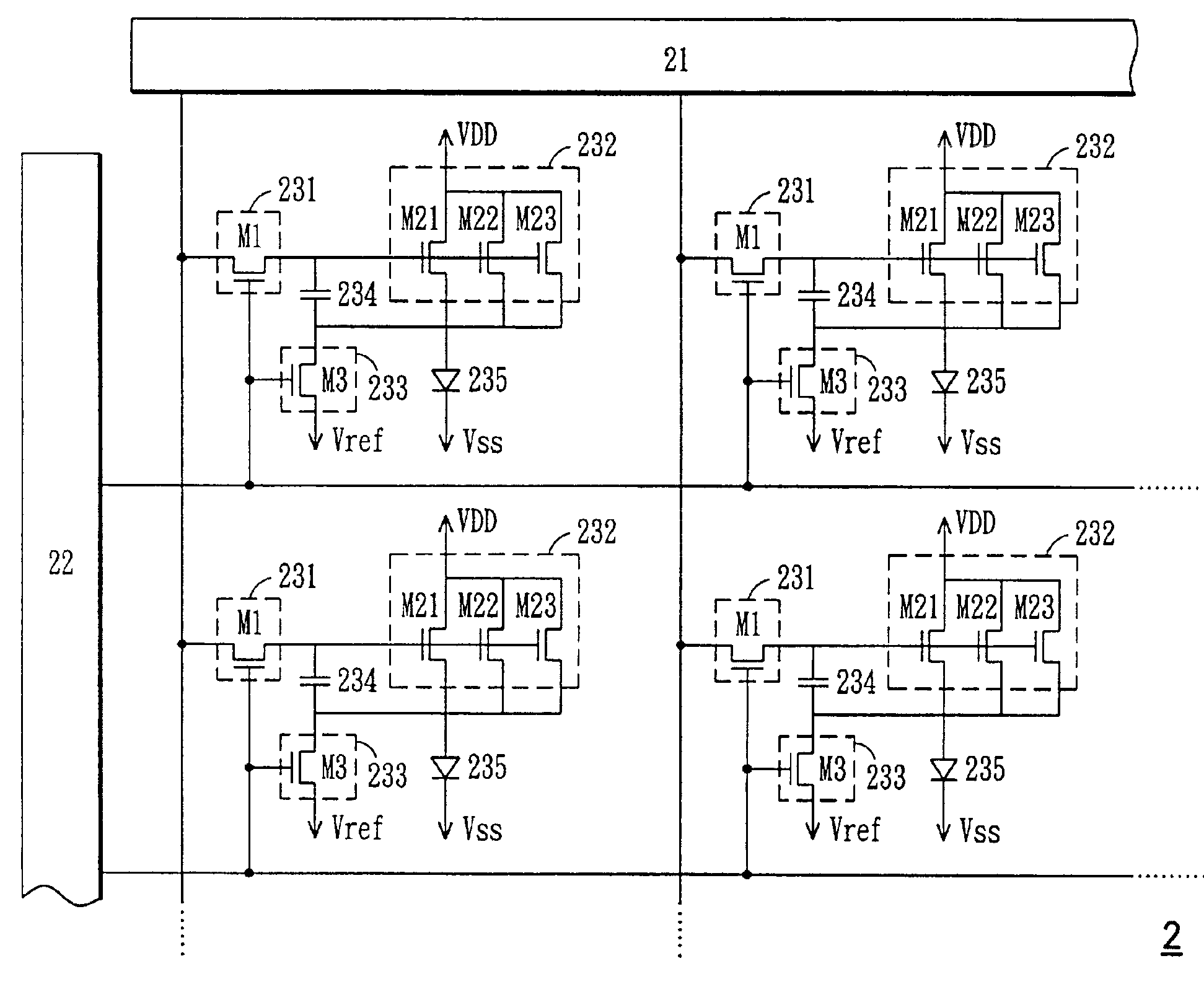
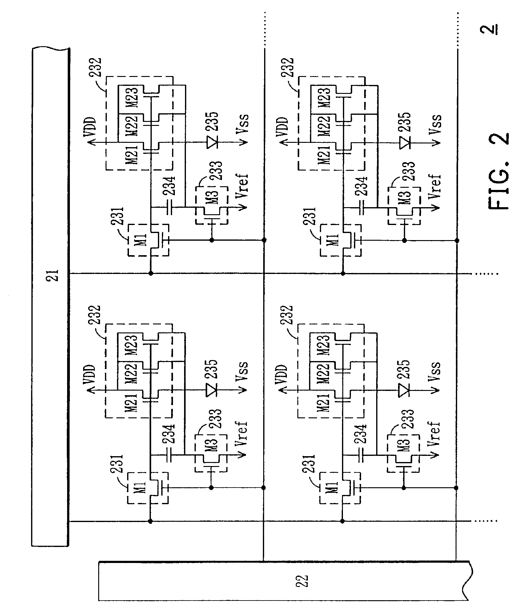
[0014]FIG. 2 is a diagram showing a display driving circuit according to one embodiment of the invention. The driving circuit 2 comprises a data electrode 21, a scan electrode 22 and a display cell composed of switches 231, 232, 233, capacitor 234 and light emitting diode 235. The light emitting diode 235 may be an OLED or PLED. For clarity, there are only four display cells shown in FIG. 2. A data signal and scan signal are output from the data electrode 21 and scan electrode 22 respectively. In each of the display cells, the cathode of the light emitting diode 235 is coupled to a power supply (not shown) providing a first voltage Vss. The voltage Vss is a negative voltage. Thus, the cathode of the light emitting diode 235 receives a negative voltage Vss. A first end of the first switch 231 is coupled to the data electrode 21 to receive the data signal. A second end of the first switch 231 is coupled to a third end of the second switch 232 and to a first end of capacitor 234. A fir...


PUM


Abstract

A display driving circuit. The circuit comprises a first electrode from which a data signal is output, a second electrode from which a scan signal is output, a capacitor having a first and second end with a voltage difference therebetween, a light emitting diode having an anode and cathode coupled to a first power supply providing a first voltage(Vss), a first switch having a first end coupled to the first electrode to receive the data signal and a second end coupled to the first end of the capacitor, a second switch having a first end coupled to a second power supply providing a second voltage(VDD) and a second end coupled to the anode of the light emitting diode, and a third switch having a first end coupled to a third power supply providing a third voltage(Vref) and a second end coupled to the second end of the capacitor.

Description

BACKGROUND OF THE INVENTION[0001]1. Field of the Invention[0002]The present invention relates to a circuit for a display, particularly to a driving circuit for an active matrix display, which includes amorphous-Si TFTs.[0003]2. Description of the Prior Art[0004]FIG. 1 is a diagram showing a conventional display driving circuit. The driving circuit 1 comprises a data electrode 11, a scan electrode 12 and a display cell composed of transistors 131, 132, capacitor 134 and light emitting diode 133. For clarity, there are only four display cells shown in FIG. 1. A data signal and scan signal are output from the data electrode 11 and scan electrode 12 respectively. In each of the display cells, the transistor 131 is turned on by the scan signal received by the gate, whereby the data signal is transferred to the gate of the transistor 132 through the transistor 131. There is a voltage difference generated by the data signal and stored on the capacitor 134. This voltage difference determine...

Claims


Application Information

Patent Timeline
IPC IPC(8): G09G3/32H01L27/32
CPCG09G3/3233G09G2300/0417G09G2300/0809G09G2300/0842H01L27/3244H10K59/12
Inventor SUNG, CHIH-FENGLEE, HSIN-HUNG
Owner AU OPTRONICS CORP
Why Eureka
Try Eureka