Design techniques for analyzing integrated circuit device characteristics

a design technique and integrated circuit technology, applied in the direction of cad circuit design, program control, instruments, etc., can solve the problems of increasing the difficulty of providing adequate power distribution, the noise condition of the chip due to switching activity on the chip has become a major new challenge, etc., to improve the analysis capability of the integrated circuit device's characteristics, reduce memory and processor utilization, and improve the effect of the analysis capability

Inactive Publication Date: 2005-09-27
IBM CORP
View PDF2 Cites 12 Cited by
  • Summary
  • Abstract
  • Description
  • Claims
  • Application Information

AI Technical Summary

Benefits of technology

[0006]An improved method and system for integrated circuit device physical design and layout. The physical layout of the integrated circuit device is optimally stored in a database to provide improved analysis capabilities of the integrated circuit device's characteristics. The method and system evaluates local interactions between functional blocks and decoupling cells on a given floor plan of a chip using this optimized database in order to reduce memory and processor utilization. Local noise is projected by using dI / dt and capacitance estimates. Areas of highest noise concern are identified, and floorplan mitigation actions are taken by tuning the placement of neighboring decoupling cells and their properties. Upon several iterative cycles, a near optimal solution for a given floorplan of the total chip is achieved.

Problems solved by technology

As the trend of integrating more functions in a single high performance integrated circuit device (also called a chip) continues, the on-chip noise condition due to switching activity on the chip has become a major new challenge.
In addition, as the power density increases with each technology generation (for example, 0.25 micron line widths, 0.18 micron line widths, 0.13 micron line widths, etc.), it becomes increasingly difficult to provide adequate power distribution when the power grid structure is shrinking at a similar rate to that of the power consuming gates / transistors.

Method used


Image

  • Design techniques for analyzing integrated circuit device characteristics
  • Design techniques for analyzing integrated circuit device characteristics
  • Design techniques for analyzing integrated circuit device characteristics

Examples


Embodiment Construction

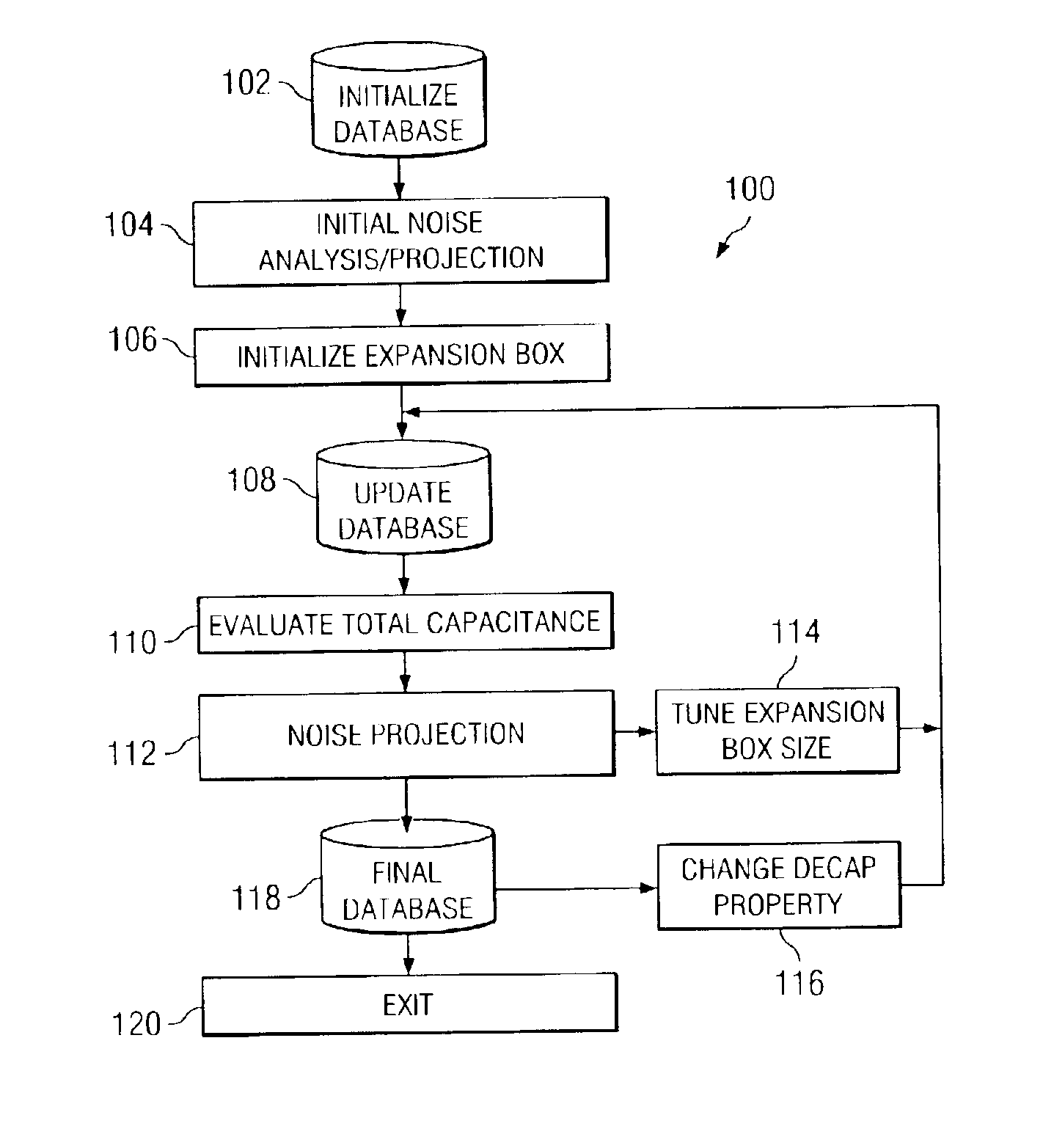
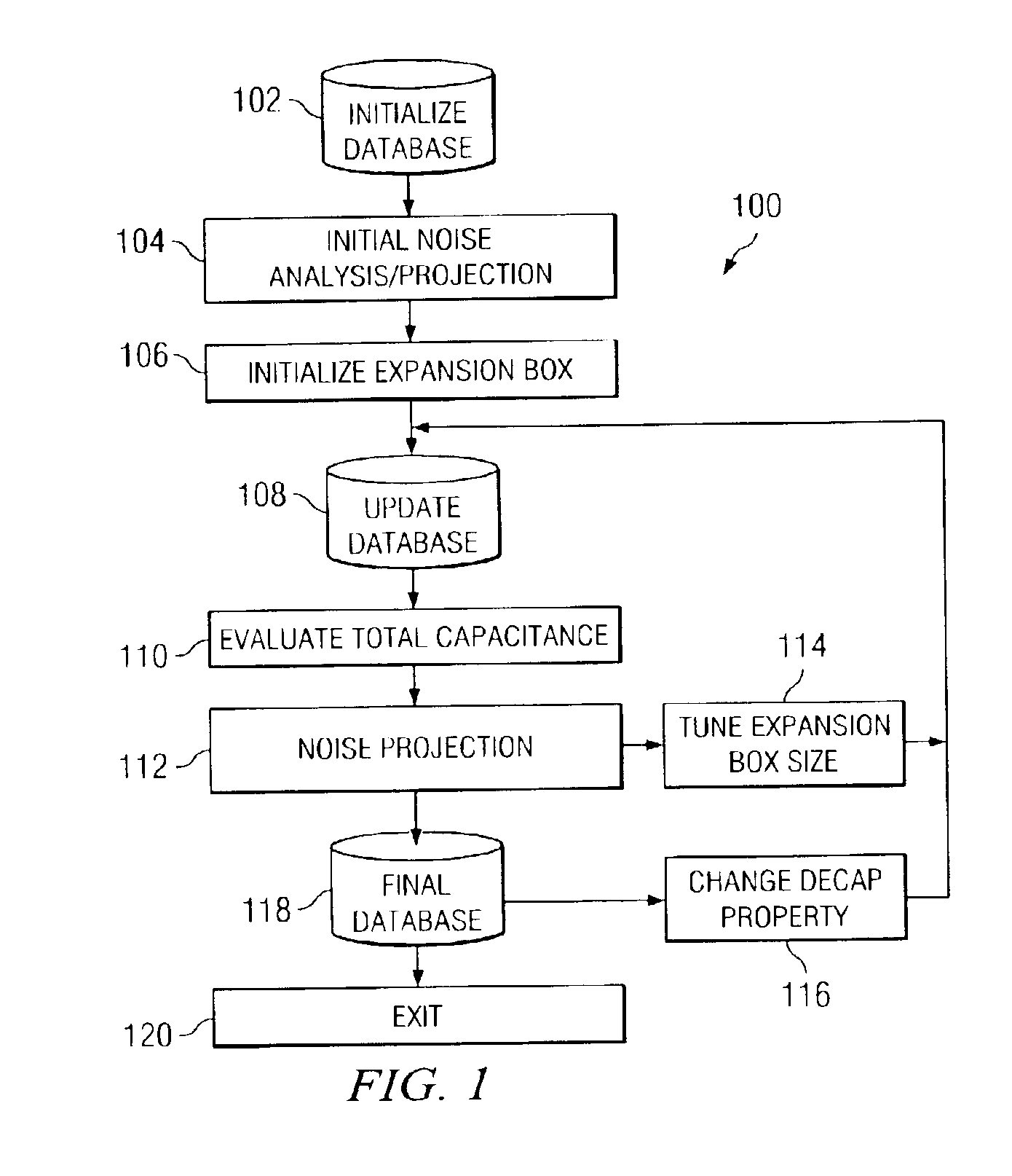
[0019]The method and procedure for improving noise characteristics of an integrated circuit device is shown generally at 100 in FIG. 1. The database is initialized at 102 with initial information, including chip level floor plan information such as size and position of all objects, macro specific data such as current signature and intrinsic capacitance of the macro, and decoupling capacitor (decap) properties such as capacitance and response time. Using the above described initial database information, the intrinsic noise level for the device is projected at 104. Each macro for the chip is given an initial expansion / boundary box size at 106. The expansion / boundary box is a variable-sized, logical perimeter around the physical macro, as will be further described below. Database 108 is used to evaluate the total capacitance for each boundary box at 110. In similar fashion to the initial noise analysis done at 104, the noise for each boundary box and its associated capacitance is proje...


PUM


Abstract

An improved method and system for integrated circuit device physical design and layout. The physical layout of the integrated circuit device is optimally stored in a database to provide improved analysis capabilities of the integrated circuit device's characteristics. The method and system evaluates local interactions between functional blocks and decoupling cells on a given floor plan of a chip using this optimized database in order to reduce memory and processor utilization. Local noise is projected by using dI/dt and capacitance estimates. Areas of highest noise concern are identified, and floor plan mitigation actions are taken by tuning the placement of neighboring decoupling cells and their properties. Upon several iterative cycles, a near optimal solution for a given floor plan of the total chip is achieved.

Description

BACKGROUND OF THE INVENTION[0001]1. Technical Field[0002]The present invention relates to integrated circuit device design, and more particularly to integrated circuit design techniques to mitigate on-chip noise of such device.[0003]2. Description of Related Art[0004]Improvements in manufacturing processes are enabling integrated circuit devices to offer more functionality as the size of individual transistors contained therein get smaller and smaller, thus allowing more transistors to be packaged within an integrated circuit device. As the trend of integrating more functions in a single high performance integrated circuit device (also called a chip) continues, the on-chip noise condition due to switching activity on the chip has become a major new challenge. In addition, as the power density increases with each technology generation (for example, 0.25 micron line widths, 0.18 micron line widths, 0.13 micron line widths, etc.), it becomes increasingly difficult to provide adequate p...

Claims


Application Information

Patent Timeline
Patent Type & Authority Patents(United States)
IPC IPC(8): G06F17/50
CPCG06F17/5036G06F17/5068G06F30/367G06F30/39
Inventor CLABES, JOACHIM GERHARDHARIDASS, ANANDWANG, MICHAEL F.
Owner IBM CORP
Why Eureka
Try Eureka