Grooved polishing pad and method

a polishing pad and groove technology, applied in the field of polishing, can solve the problems of increased defectivity, non-uniform polishing, and detrimental to polishing, and achieve the effects of improving polishing efficiency, improving polishing efficiency, and improving polishing efficiency

Active Publication Date: 2005-10-18
ROHM & HAAS ELECTRONICS MATERIALS CMP HLDG INC
View PDF13 Cites 43 Cited by
  • Summary
  • Abstract
  • Description
  • Claims
  • Application Information

AI Technical Summary

Problems solved by technology

Mixing wakes can be detrimental to polishing for a number of reasons, such as non-uniform polishing and increased defectivity.

Method used


Image

  • Grooved polishing pad and method
  • Grooved polishing pad and method
  • Grooved polishing pad and method

Examples


Embodiment Construction

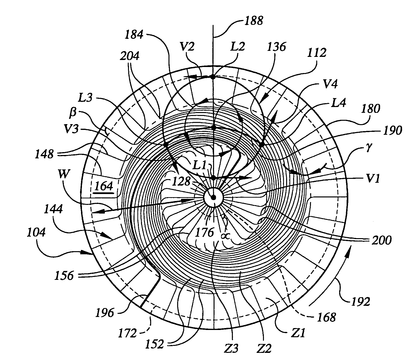
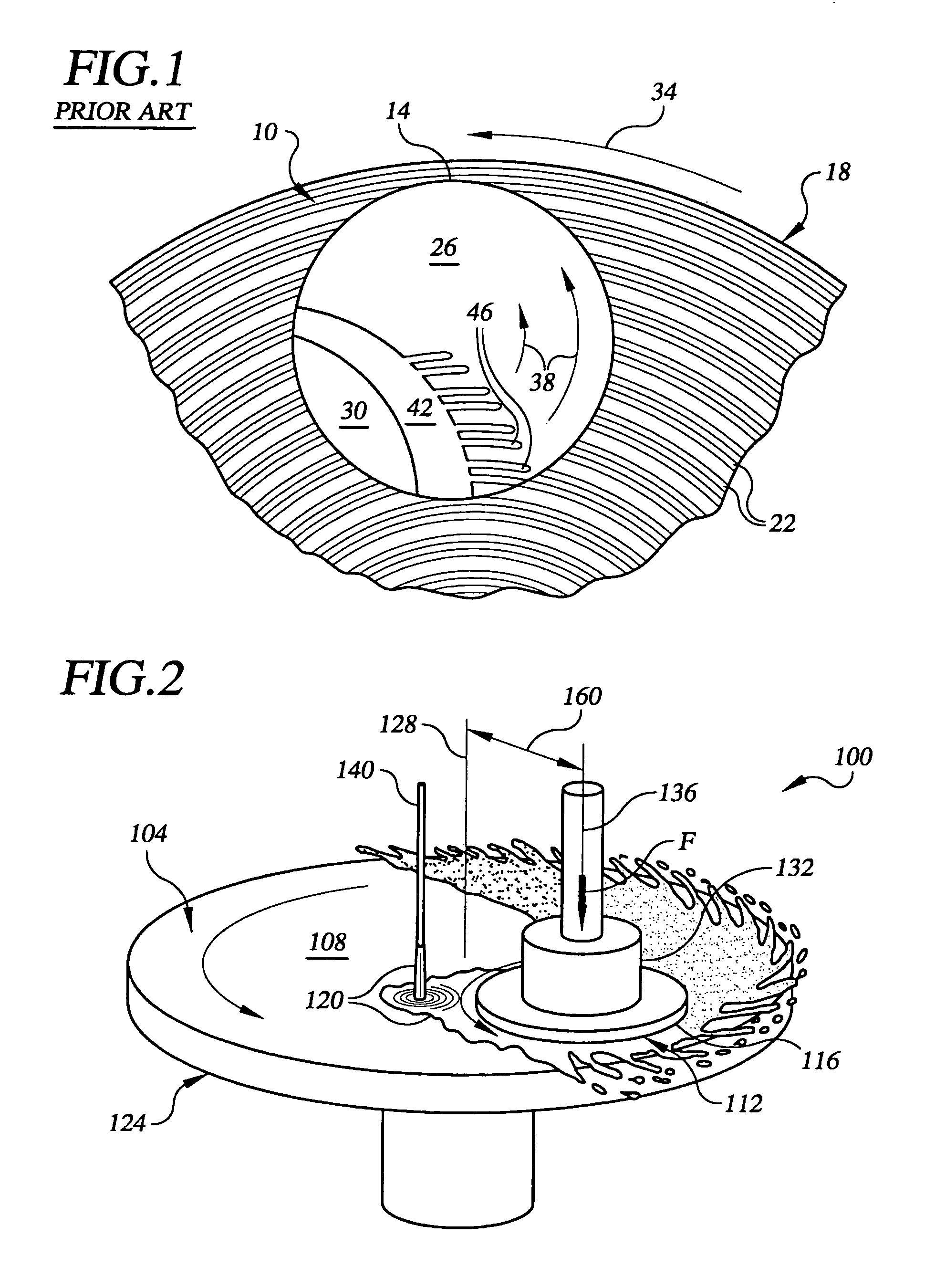
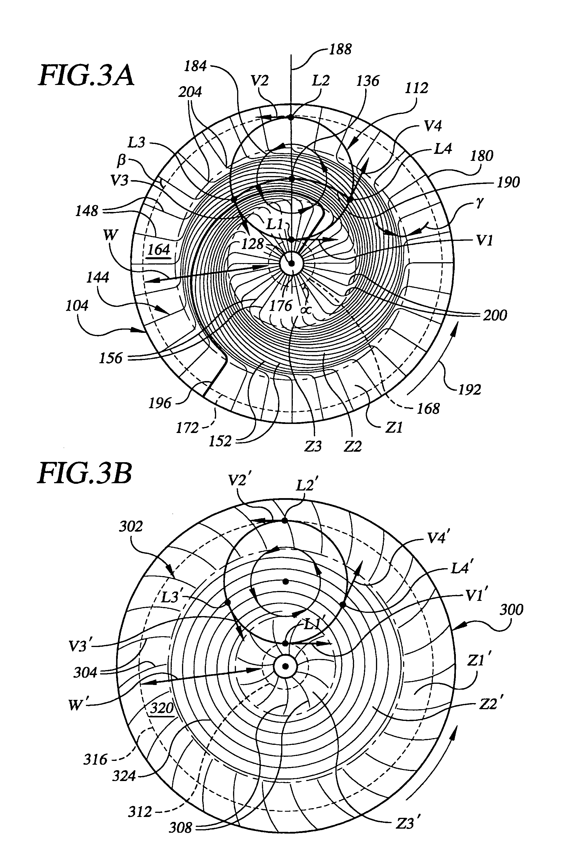
[0016]Referring again to the drawings, FIG. 2 generally illustrates the primary features of a dual-axis chemical mechanical polishing (CMP) polisher 100 suitable for use with the present invention. Polisher 100 generally includes a polishing pad 104 having a polishing layer 108 for engaging an article, such as semiconductor substrates, including semiconductor wafer 112 (processed or unprocessed); optical substrates including glass and flat panel displays; and substrates for storing magnetic information, including nickel disks, so as to effect polishing of the polished surface 116 of the workpiece in the presence of a slurry 120 or other polishing medium. For the sake of convenience, the terms “wafer” and “slurry” are used below without the loss of generality. In addition, as used in this specification, including the claims, the terms “polishing medium” and “slurry” include particle-containing polishing solutions and non-particle-containing solutions, such as abrasive-free and reacti...


PUM

PropertyMeasurementUnit
angleaaaaaaaaaa
angleaaaaaaaaaa
pressureaaaaaaaaaa

Abstract

A polishing pad (104, 300, 400, 500) for polishing a wafer (112, 516), or other article. The polishing pad includes a polishing layer (108) having a polishing region (164, 320, 420, 504) defined by first and second boundaries ((168, 172), (312, 316), (412, 416) (508, 512)) having shapes and locations that are a function of the size of polished surface (116) of the article being polished and the type of polisher (100) used. The polishing region has several zones ((Z1–Z3) (Z1′–Z3′)(Z1″–Z3″)(Z1′″–Z3′″)) each containing corresponding grooves ((148, 152, 156)(304, 308, 324)(404, 408, 424)(520, 524, 528)) having orientations selected based on the direction of one or more velocity vectors (V1–V4)(V1′–V4′)(V1″–V4″) (V′″–V4′″) of the wafer in that zone.

Description

BACKGROUND OF THE INVENTION[0001]The present invention generally relates to the field of polishing. In particular, the present invention is directed to a polishing pad having a groove pattern for reducing slurry mixing wakes in the grooves.[0002]In the fabrication of integrated circuits and other electronic devices, multiple layers of conducting, semiconducting and dielectric materials are deposited onto and etched from a surface of a semiconductor wafer. Thin layers of conducting, semiconducting and dielectric materials may be deposited by a number of deposition techniques. Common deposition techniques in modern wafer processing include physical vapor deposition (PVD), also known as sputtering, chemical vapor deposition (CVD), plasma-enhanced chemical vapor deposition (PECVD) and electrochemical plating. Common etching techniques include wet and dry isotropic and anisotrdpic etching, among others.[0003]As layers of materials are sequentially deposited and etched, the uppermost surf...

Claims


Application Information

Patent Timeline
Patent Type & Authority Patents(United States)
IPC IPC(8): B24B37/04B24D13/00B24D13/14B24B37/00H01L21/304
CPCB24B37/26Y10S451/921F25B21/02F25B2313/003F25B2321/023
Inventor MULDOWNEY, GREGORY P.
Owner ROHM & HAAS ELECTRONICS MATERIALS CMP HLDG INC
Why Eureka
Try Eureka