Semiconductor-processing reaction chamber

a reaction chamber and semiconductor technology, applied in the direction of electrolysis components, vacuum evaporation coatings, coatings, etc., can solve the problems of pin bindage, pin bindage, and semiconductor wafer back contamination, etc., to achieve the effect of stabilizing the rise and the lower of the semiconductor wafer

Inactive Publication Date: 2005-10-18
ASM JAPAN
View PDF41 Cites 205 Cited by
  • Summary
  • Abstract
  • Description
  • Claims
  • Application Information

AI Technical Summary

Benefits of technology

[0010]One preferred embodiment of the present invention provides a reaction chamber with substrate-supportin

Problems solved by technology

In ultrafine and high-density semiconductor devices, particle contamination on the back of the semiconductor wafer is

Method used


Image

  • Semiconductor-processing reaction chamber
  • Semiconductor-processing reaction chamber
  • Semiconductor-processing reaction chamber

Examples


Embodiment Construction

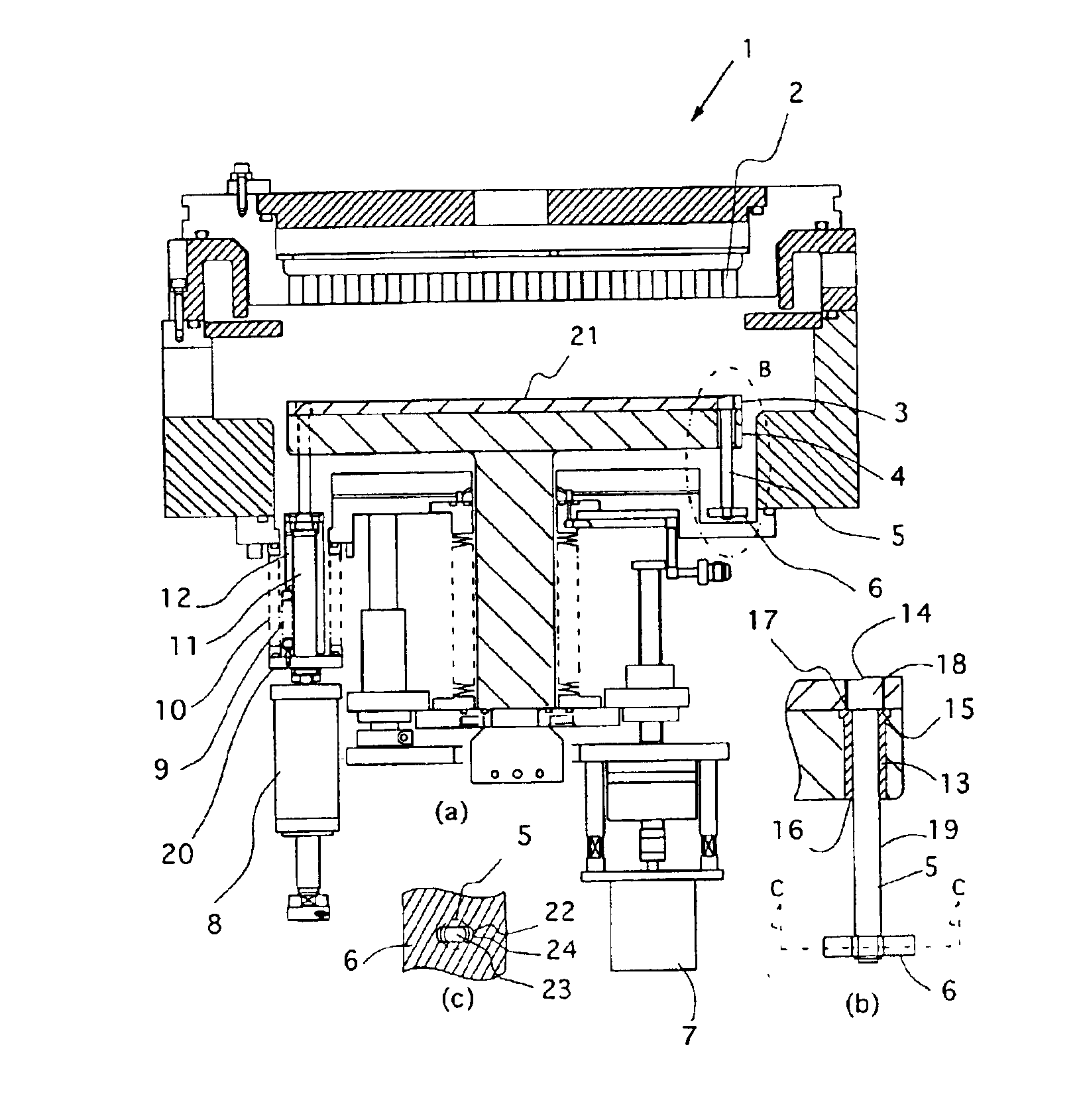
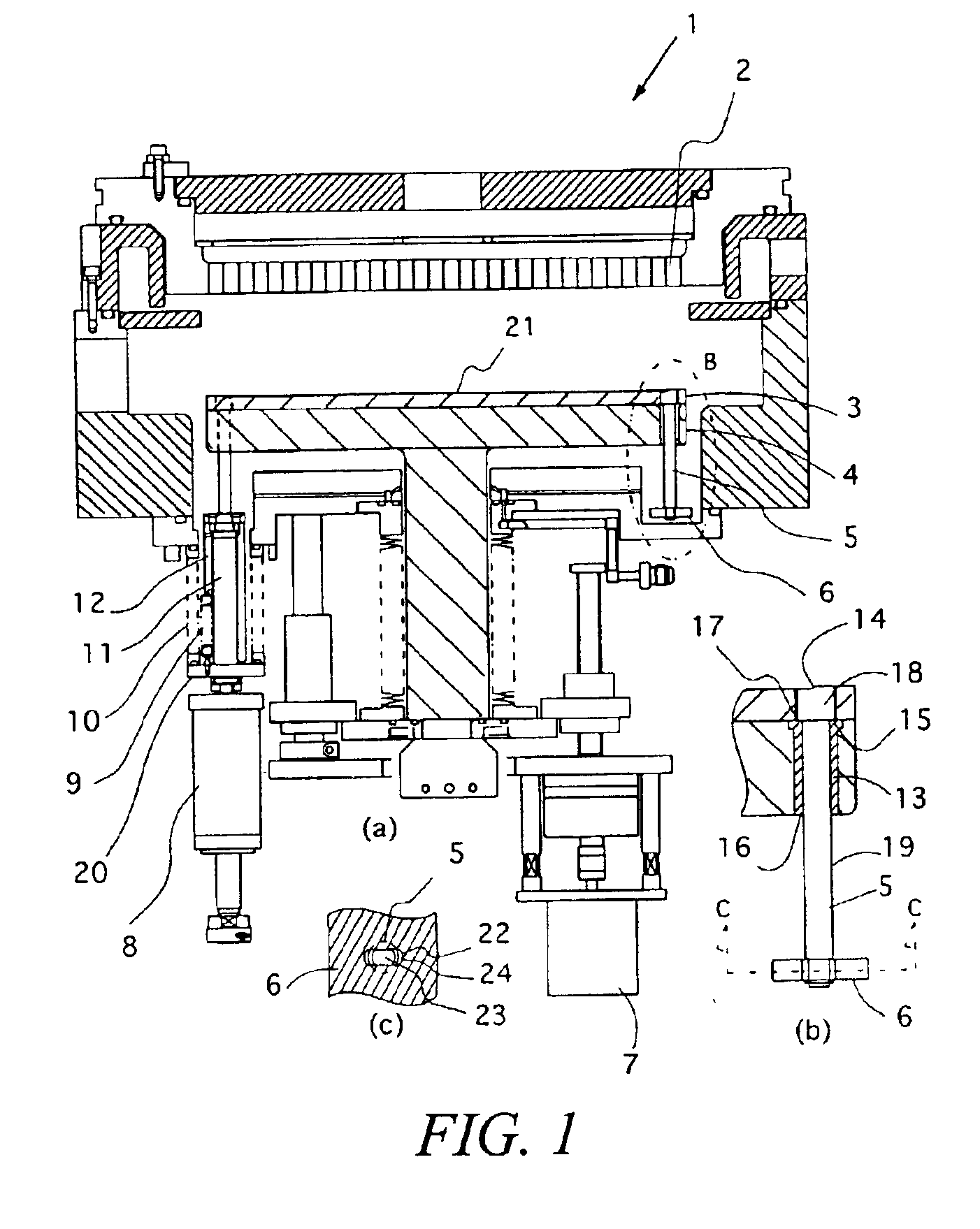
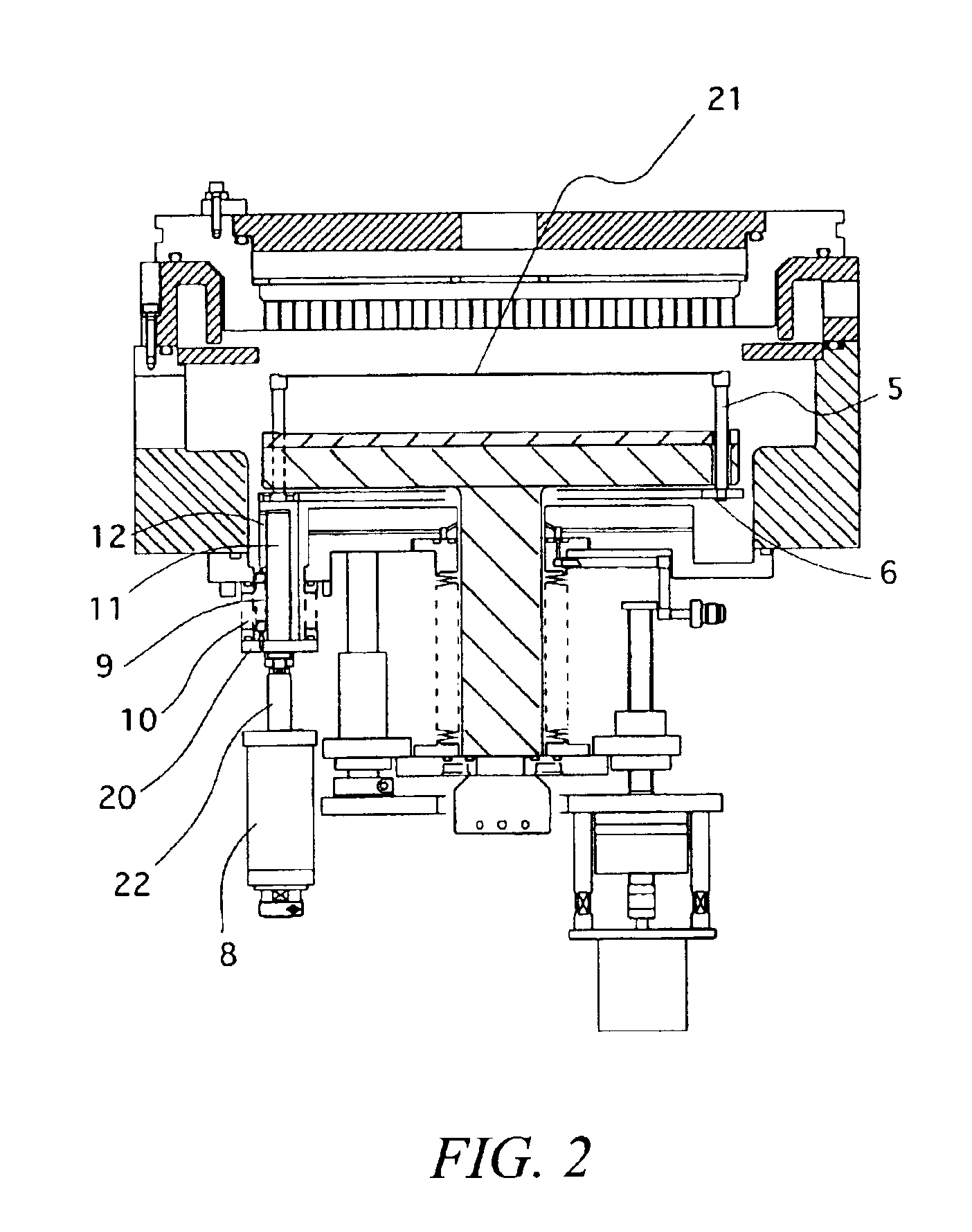
[0027]The present invention is described in detail by reference to the accompanying figures. FIG. 1(a) provides a cross section of a preferred embodiment of a reaction chamber according to the present invention. FIG. 1(b) is a detail view of area “B” of FIG. 1(a). Inside the reaction chamber 1, a disk-shaped susceptor 4 for supporting a semiconductor wafer is provided. Above the susceptor 4, a shower plate 2 for emitting a jet of reaction gas toward the semiconductor wafer is provided facing the susceptor 4. In plasma-enhanced CVD (PECVD), both the susceptor and the shower plate comprise electrodes of a high-frequency power source. The susceptor 4 is raised and lowered by a susceptor drive motor 7. During the deposition process, the susceptor 4 is raised to provide a reduced reaction area (see FIG. 3).

[0028]On the surface of the susceptor 4, a top plate 3 having about the same diameter as the susceptor is installed. The top plate 3 is preferably made of ceramic or aluminum. In an al...


PUM

PropertyMeasurementUnit
Thermal expansion coefficientaaaaaaaaaa

Abstract

The present application provides a PECVD reaction chamber for processing semiconductor wafers comprising a susceptor for supporting a semiconductor wafer inside the reaction chamber wherein the susceptor comprises a plurality vertical through-bores, a moving means for moving the susceptor vertically between at least a first position and a second position, wafer-lift pins passing through the through-bores wherein the lower end of each wafer pin is attached to a lift member, and a lift member linked with an elevating mechanism for moving the wafer-lift pins vertically. The disclosed apparatus reduces contamination on the underside of the semiconductor wafer.

Description

TECHNICAL FIELD OF THE INVENTION[0001]The present application relates to a reaction chamber for processing semiconductor wafers, and in particular, to wafer-supporting pins for lifting semiconductor wafers inside a reaction chamber.BACKGROUND OF THE INVENTION[0002]Currently, most semiconductor processing devices are single-wafer-devices processing type devices which process semiconductor wafers sheet by sheet. These single-wafer-processing type devices generally possess a susceptor inside a reaction chamber on which processing is performed while heating semiconductor wafers at a given temperature on the susceptor.[0003]A typical susceptor in a single-wafer-processing type device comprises a disc-shaped body made of metal or ceramic having high heat conductivity, and has a built-in heating element such as an electric heater. This type of susceptor has at least three through-bores into which substrate-supporting pins are inserted vertically such that the pins can move freely. When an ...

Claims


Application Information

Patent Timeline
IPC IPC(8): C23C16/458H01L21/687H01L21/67H01L21/683
CPCC23C16/4583H01L21/68742
Inventor YAMAGISHI, TAKAYUKI
Owner ASM JAPAN
Why Eureka
Try Eureka