Semiconductor device having standby mode and active mode

a technology of active mode and semiconductor device, which is applied in the direction of semiconductor devices, digital storage, instruments, etc., can solve the problems of large power consumption when a potential is applied, unstable disadvantageous increase of load capacitance of internal power supply potential vdds, etc., to suppress a standby current to be low, and stable raise an internal power supply potential

Inactive Publication Date: 2006-04-04
RENESAS ELECTRONICS CORP
View PDF12 Cites 9 Cited by
  • Summary
  • Abstract
  • Description
  • Claims
  • Application Information

AI Technical Summary

Benefits of technology

[0023]It is, therefore, a main object of the present invention to provide a semiconductor device capable of stably raising ...

Problems solved by technology

However, if internal power supply potential VDDS is lowered to approximately 1.2 to 1.5 V, it is difficult for VBL generation circuit 150 shown in FIG. 30 to generate bit line precharge potential VBL.
Nevertheless, if VBL generation circuit 160 is employed, the load capacitance of internal power supply potential VDDS disadvantageously increases, making internal power supply potential VDDS unstable.
However, if internal power supply potential VDDS is used as a current supply source for the VBL gene...

Method used


Image

  • Semiconductor device having standby mode and active mode
  • Semiconductor device having standby mode and active mode
  • Semiconductor device having standby mode and active mode

Examples


first embodiment

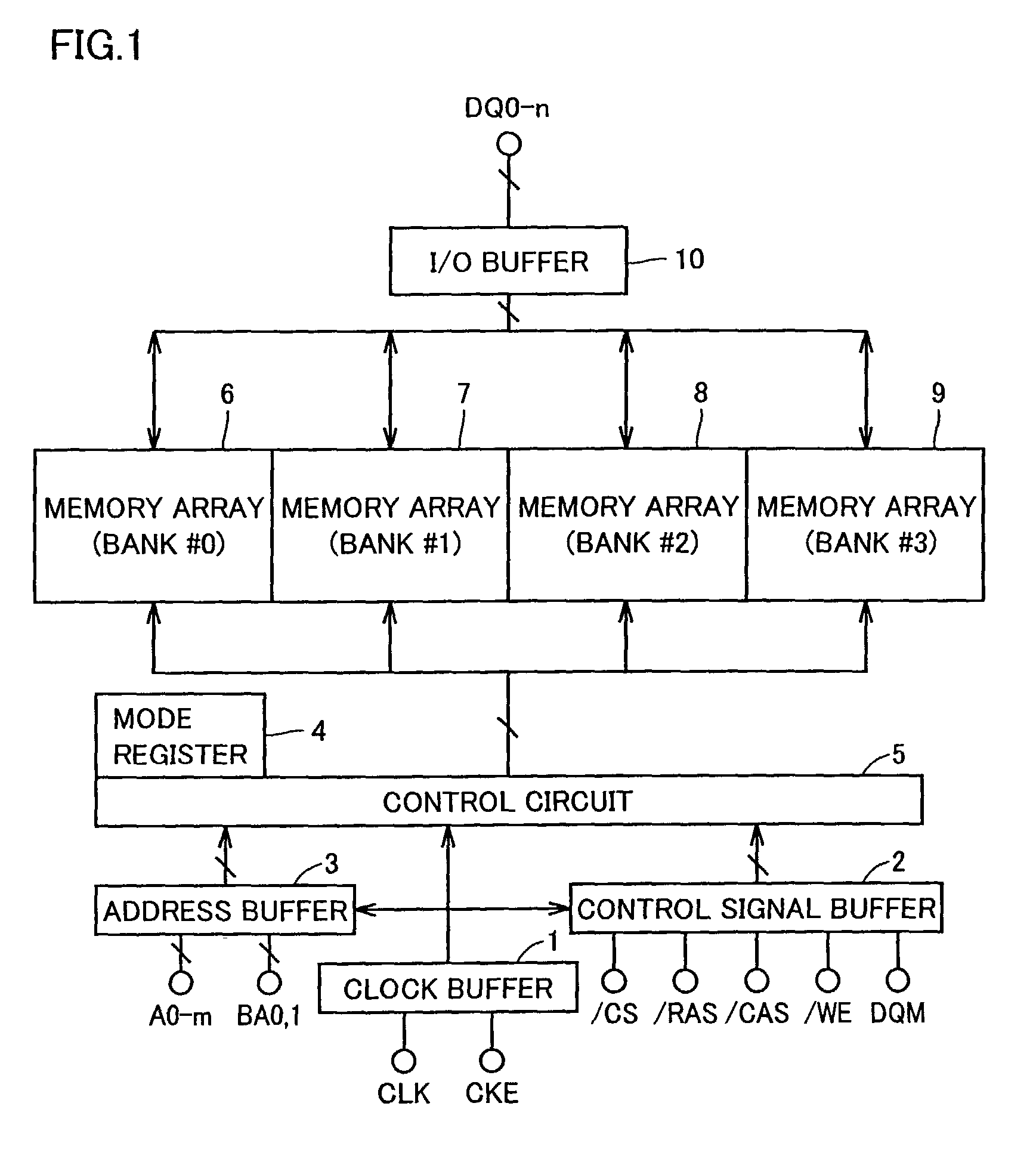
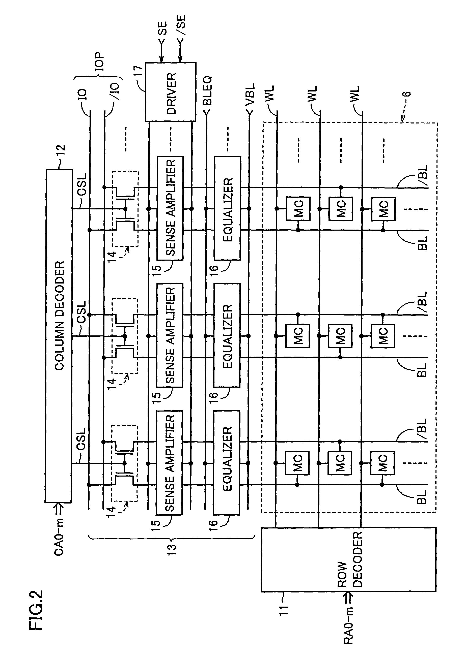
[0058]FIG. 1 is a block diagram which shows the schematic configuration of a synchronous DRAM (referred to as “SDRAM” hereinafter) in the first embodiment according to the present invention. In FIG. 1, SDRAM includes a clock buffer 1, a control signal buffer 2, an address buffer 3, a mode register 4, a control circuit 5, four memory arrays 6 to 9 (banks #0 to #3) and an I / O buffer 10.

[0059]Clock buffer 1 is activated by an external control signal CKE, and transmits an external clock signal CLK to control signal buffer 2, address buffer 3 and control circuit 5. Control signal buffer 2 latches external control signals / CS, / RAS, / CAS, / WE and DQM synchronously with external clock signal CLK from clock buffer 1, and applies these control signals to control circuit 5. Address buffer 3 latches external address signals A0 to Am (where 0 is an integer not smaller than 0) and bank select signals BA0 and BA1 synchronously with external clock signal CLK from clock buffer 1, and applies these ...

second embodiment

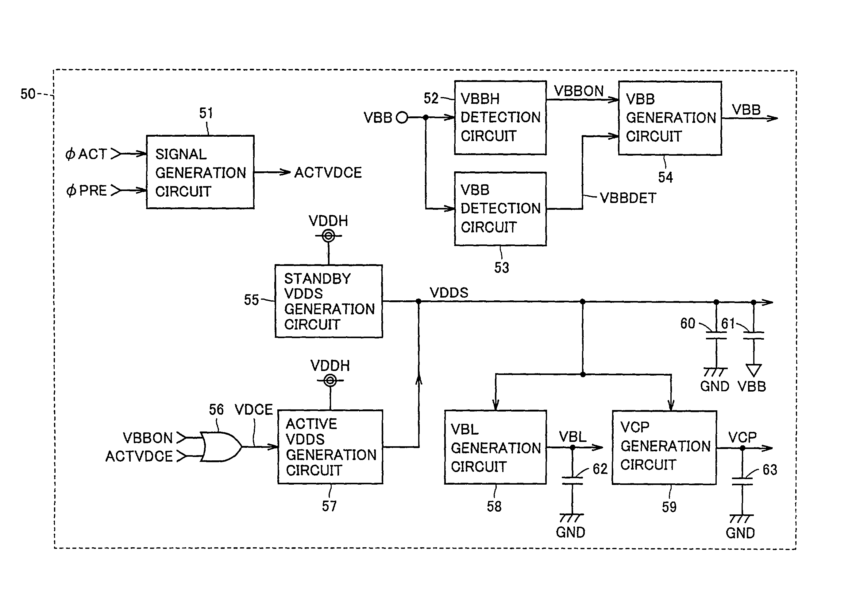
[0096]FIG. 13 is a circuit block diagram which shows the important parts of the internal potential generation circuit of SDRAM in the second embodiment according to the present invention. Referring to FIG. 13, this internal potential generation circuit differs from that shown in FIG. 12 in that a POR generation circuit 80 and a signal generation circuit 81 are added.

[0097]As shown in FIG. 14, POR generation circuit 80 includes a resistance element 82 and N-channel MOS transistors 83 and 84 which are connected in series between an external power supply potential VDDH line and a ground potential GND line, and an inverter 85. The gate of N-channel MOS transistor 83 receives external power supply potential VDDH. The gate of N-channel MOS transistor 84 is connected to the drain thereof. N-channel MOS transistor 84 constitutes a diode element. A signal which appears at a node N82 between resistance element 82 and N-channel MOS transistor 83 is inverted by inverter 85 and become a power-on...

third embodiment

[0106]Signal generation circuit 81 in the second embodiment is a circuit which sets signal SDVCE at “H” level only during a period after the level of signal ZPOR is raised to “H” level and extending until signal VBBDET is lowered to “L” level. Therefore, as shown in FIG. 17, if the operation of VBB detection circuit 53 becomes unstable and signal VBBDET rings between “H” level and “L” level, then the period in which signals STVDCE and VCDCE are at “H” level becomes short, so that the time period in which active VDDS generation circuit 57 is activated becomes short and internal power supply potential VDDS and negative potential VBB change greatly, as in the case of the conventional art. The third embodiment is intended to solve these disadvantages.

[0107]FIG. 18 is a circuit block diagram which shows the important parts of the internal potential generation circuit of SDRAM in the third embodiment according to the present invention. Referring to FIG. 18, this internal potential generat...


PUM


Abstract

An internal potential generation circuit of an SDRAM includes a standby VDDS generation circuit which has a relatively low current driving force and which generates an internal power supply potential, and an active VDDS generation circuit which has a relatively high current driving force, which is activated during a period after an external power supply potential is applied until a negative potential reaches a threshold potential, and in an activation period, and which generates the internal power supply potential. Therefore, it is possible to raise the internal power supply potential stably without increasing standby current when the power supply is turned on.

Description

BACKGROUND OF THE INVENTION[0001]1. Field of the Invention[0002]The present invention relates to a semiconductor device, and more particularly to a semiconductor device which has a standby mode and an active mode.[0003]2. Description of the Background Art[0004]Conventionally, an eDRAM on which a logic circuit and a DRAM are embedded on the same chip has a dual-oxide structure. In the dual-oxide structure, a circuit driven by an external power supply voltage VDDH, which is a relatively high voltage, for a DRAM, consists of thick film transistors, and a circuit driven by a power supply voltage, which is a relatively low voltage for a logic circuit, consists of thin film transistors. In addition, an external power supply voltage VDDH is lowered to generate an internal power supply voltage VDDS for sense amplifiers, a bit line precharge voltage VBL=VDDS / 2 is generated from internal power supply voltage VDDS, and each sense amplifier consists of thin film transistors to accelerate operat...

Claims


Application Information

Patent Timeline
IPC IPC(8): G11C7/00G11C11/407G11C7/06G11C11/4074G11C11/4076H01L27/02H01L27/108
CPCG11C7/065G11C11/4074G11C11/4076H01L27/10897G11C2207/2227H01L27/0214H10B12/50
Inventor AKIYAMA, MIHOKOMORISHITA, FUKASHI
Owner RENESAS ELECTRONICS CORP
Why Eureka
Try Eureka