

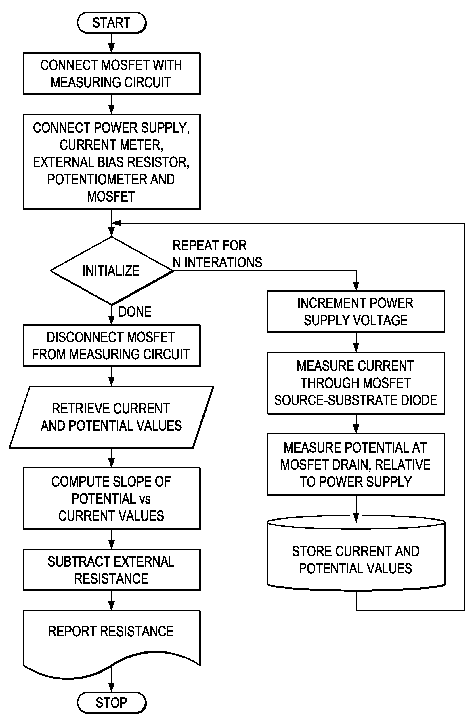
Method to accurately estimate the source and drain resistance of a MOSFET
a technology of mos transistor and source and drain resistance, which is applied in the field of integrated circuits, can solve the problems of increasing the cost and complexity of transistor testing, affecting the accuracy of mos transistor estimation, and unable to be repeated,
- Summary
- Abstract
- Description
- Claims
- Application Information
AI Technical Summary
Benefits of technology
Problems solved by technology
Method used
Image

Examples
Embodiment Construction
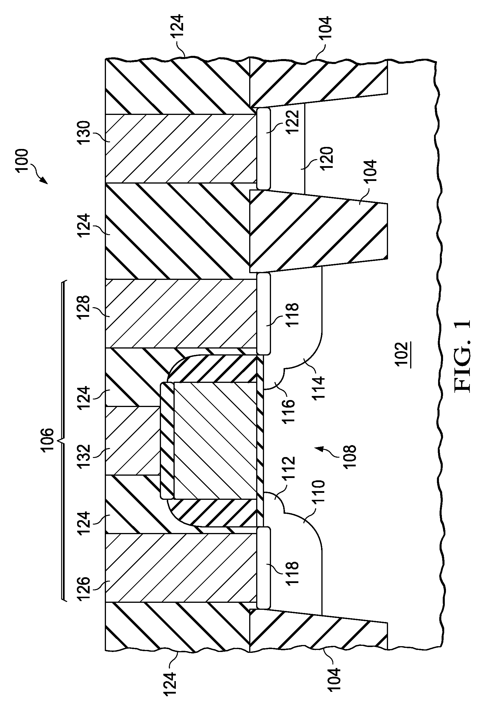
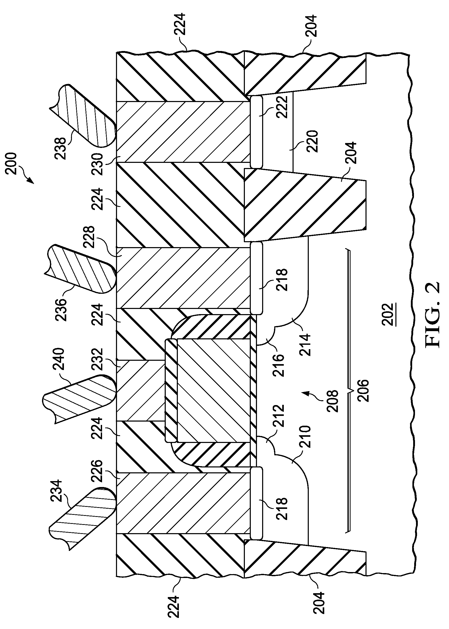
[0012]FIG. 1 is a cross-section of a MOS transistor, fabricated on an integrated circuit containing MOS transistors, being measured per this invention. Integrated circuit (100) comprises substrate (102), isolation structures (104), typically formed by local oxidation of silicon (LOCOS) or shallow trench isolation (STI) process, and typically composed of silicon dioxide, and transistor (106). Transistor (106) is further comprised of gate structure (108), source (110), source extension (112), drain (114) and drain extension (116). Source and drain regions may have metal silicide (118) on top surfaces to reduce resistance. The substrate region (102) is contacted through an optional diffused layer (120) and optional metal silicide layer (122). A layer or layers of dielectric material or materials (124), known as the pre-metal dielectric (PMD), is deposited over the transistors and exposed substrate regions. Metal contacts are formed through the PMD to contact regions of interest on the ...
PUM
 Abstract
Description
Claims
Application Information