Semiconductor device

a semiconductor device and membrane technology, applied in the details of semiconductor/solid-state devices, semiconductor devices, electrical appliances, etc., can solve the problems of harming the semiconductor device, and achieve the effect of excellent wet-proof properties

Inactive Publication Date: 2005-11-22
ROHM CO LTD
View PDF15 Cites 24 Cited by
  • Summary
  • Abstract
  • Description
  • Claims
  • Application Information

AI Technical Summary

Benefits of technology

[0010]An object of the present invention is to provide a semiconductor device in which moisture penetrating from outside is hard to reach a semiconductor chip, and which has an excellent wet-proof property.
[0013]According to the present invention, the lower portion of the inner connecting portion of the lead frame is covered or coated with the inner connecting portion sealing resin. Therefore, at this portion, the boundary surface of the lead frame and the sealing resin is not exposed, and moisture cannot penetrate into the semiconductor device from this portion. Moisture has to travel a longer distance in order to reach the connecting portion between the inner connecting portion and the metal wire, and accordingly, the traveling distance of moisture becomes the longer in order to reach the semiconductor chip. Therefore, such a semiconductor device has an excellent wet-proof property.
[0015]The upper surface area of the supporting portion may be equal to, larger or smaller than the bottom surface area of the semiconductor chip. When the supporting portion is smaller than the semiconductor chip, a larger area of the semiconductor chip is in direct contact with the sealing resin, and thereby detachment of the semiconductor chip from the supporting portion along the boundary surface therebetween can be reduced.
[0020]Further, since the inner connecting portion sealing resin is the sealing resin having entered in the underside of the inner connecting portion, these resins are of the same kind. Consequently, these resins can be formed at the same time, thereby to improve productivity.
[0024]Such a structure of the inner connecting portion, for example, can be obtained only by machining the head of one end of the lead terminal portion. As a result, the semiconductor device according to the present invention has a simple structure and can be fabricated at a low cost.

Problems solved by technology

It has been a problem to be solved that such moisture, containing ions such as Cl−, Fe+ and Ni+, causes corrosion through chemical reaction with Al and has a harmful influence on the semiconductor device.

Method used


Image

  • Semiconductor device
  • Semiconductor device
  • Semiconductor device

Examples


first embodiment

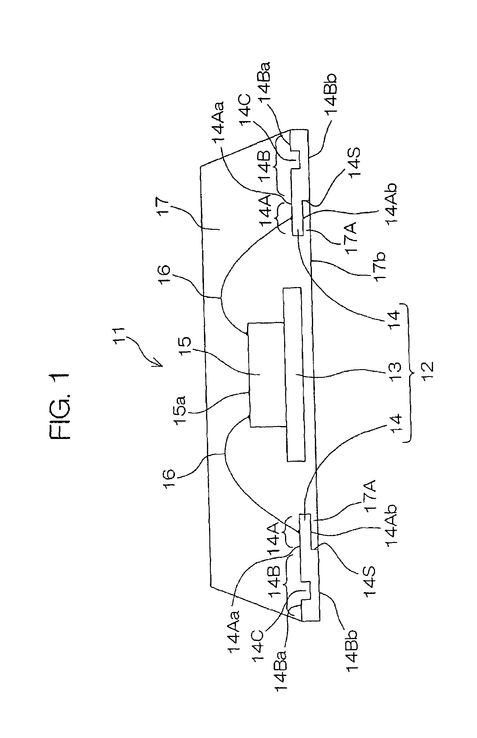
[0033]FIG. 1 is a schematic sectional view showing the structure of a semiconductor device 11 according to the present invention.

[0034]This semiconductor device 11 comprises a lead frame 12 having a supporting portion 13 and lead terminal portions 14, a semiconductor chip 15 mounted on the supporting portion 13, metal wires 16 for electrically connecting electrodes formed on the upper surface 15a of the semiconductor chip 15 and lead terminal portions 14 respectively, and a sealing resin 17 for sealing the semiconductor chip 15, metal wires 16, the supporting portions 13 and upper surface 14Aa, 14Ba of the lead terminal portions 14.

[0035]The lead frame 12 has such a structure that the supporting portion 13 is disposed in the central portion thereof, and the lead terminal portions 14 are surrounding the supporting portion 13. The lead frame 12 is upset so that the supporting portion 13 is disposed at a higher position than the lead terminal portions 14.

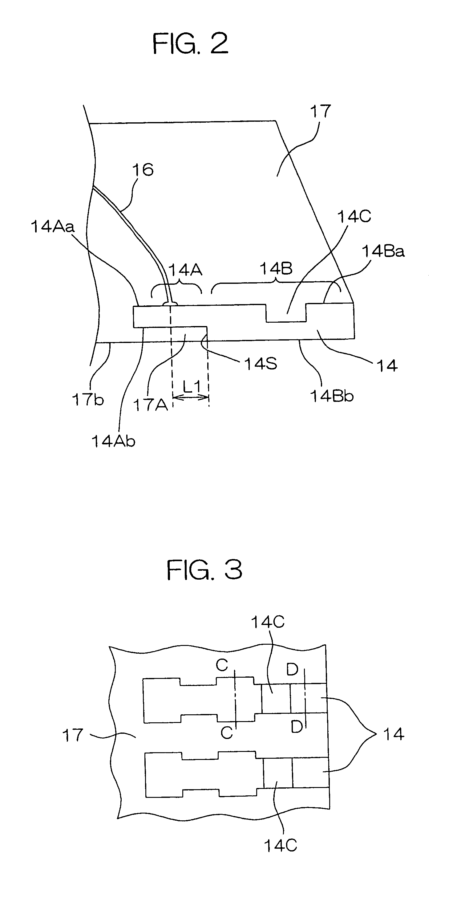
[0036]The lead terminal portion...

second embodiment

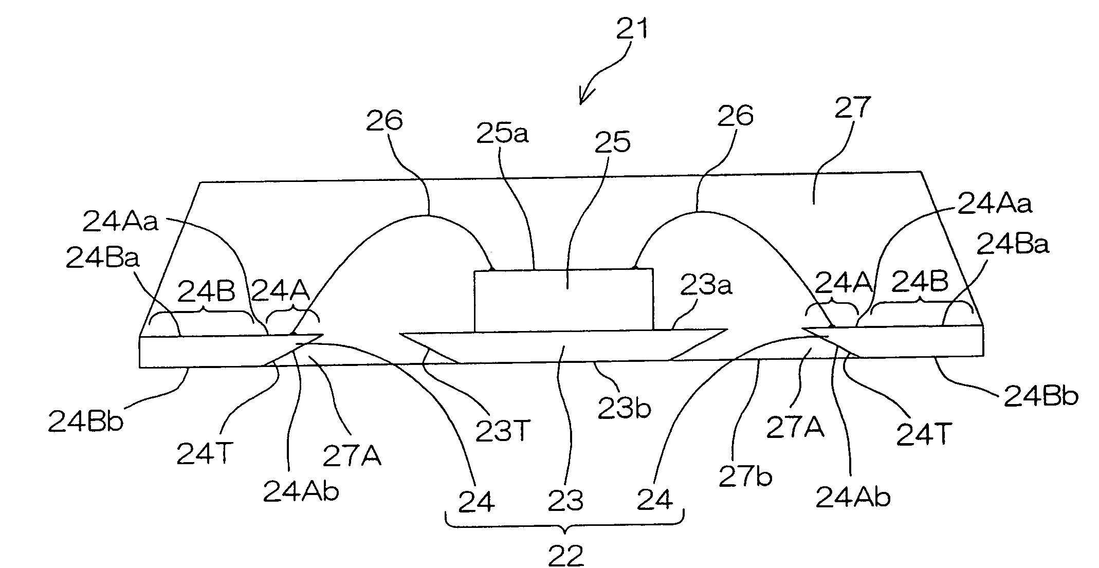
[0048]FIG. 5 is a schematic sectional view showing the structure of a semiconductor device 21 according to the present invention.

[0049]This semiconductor device 21 comprises a lead frame 22 having a supporting portion 23 and lead terminal portions 24, a semiconductor chip 25 mounted on the supporting portion 23, metal wires 26 for electrically connecting electrodes formed on the upper surface 25a of the semiconductor chip 25 and lead terminal portions 24 respectively, and a sealing resin 27 for sealing the semiconductor chip 25, metal wires 26, the upper surface 23a of the supporting portions 23 and upper surface 24Aa, 24Ba of the lead terminal portions 24.

[0050]The lead frame 22 has such a structure that the supporting portion 23 is disposed in the central portion thereof, and lead terminal portions 24 are surrounding the supporting portion 23. The supporting portion 23 and the lead terminal portions 24 are disposed at the same height.

[0051]The lead terminal portion 24 comprises an...


PUM


Abstract

A semiconductor device in which a lead frame having inner connecting portions and outer connecting portions, a semiconductor chip having electrodes on the surface thereof, and metal wires for electrically connecting electrodes on the semiconductor chip and the inner connecting portions of the lead frame are sealed with a sealing resin. The bottom side of the sealing resin of the inner connecting portion is covered with an inner connecting portion sealing resin.

Description

[0001]This is a Divisional of U.S. application Ser. No. 09 / 970,193, filed Oct. 4, 2001 now U.S. Pat. No. 6,700,189.BACKGROUND OF THE INVENTION[0002]1. Field of the Invention[0003]The present invention relates to a resin-sealed type semiconductor device in which a semiconductor chip and a part of a lead frame are sealed with a resin, and especially to a one-side sealed type semiconductor device in which a surface of a lead frame on which a semiconductor chip is mounted is sealed with a resin.[0004]2. Description of Related Art[0005]Resin-sealed type semiconductor devices in which a semiconductor chip and a part of a lead frame are sealed with a resin are widely used. Recently, as thin-type apparatus have come into general use, semiconductor devices mounted on these apparatus have also been requested to be thin-type. In conventional resin-sealed type semiconductor devices, generally both of the upper and lower portions of a semiconductor chip and a lead frame in the vicinity thereof a...

Claims


Application Information

Patent Timeline
Patent Type & Authority Patents(United States)
IPC IPC(8): H01L23/495H01L23/48H01L23/28H01L23/31H01L23/50
CPCH01L23/3107H01L23/49548H01L2224/48091H01L2224/48247H01L2924/00014H01L24/48H01L2224/451H01L24/45H01L2924/181H01L2924/00015H01L2924/00012
Inventor SHIBATA, KAZUTAKA
Owner ROHM CO LTD
Why Eureka
Try Eureka