Active optical alignment and attachment thereto of a semiconductor optical component with an optical element formed on a planar lightwave circuit

a semiconductor optical component and optical element technology, applied in the field of fiber optics, can solve the problems of difficult to achieve high-efficiency coupling, high cost of achieving proper alignment between the bulk element and the plc, and severe mechanical tolerance for adequate optical alignment in such systems

Active Publication Date: 2005-11-29
AVAGO TECH INT SALES PTE LTD
View PDF10 Cites 10 Cited by
  • Summary
  • Abstract
  • Description
  • Claims
  • Application Information

AI Technical Summary

Benefits of technology

[0009]In accordance with the present invention, a method and apparatus is provided for attaching a bulk element processing an optical beam to a PLC and optically aligning the bulk element with an optical element formed on the PLC. The method begins by securing the bulk element to a first side of a substrate. A first side of a flexure element is secured to the first side of the substrate. A second side of the flexure element is secured to a first side of the PLC on which the optical element is formed such that the bulk element and the optical element are in optical alignment to within a first level of tolerance. Subsequent to the step of securing the second side of the flexure element, a force is exerted on at least a second side of the substrate to thereby flex the flexure element. The force causes sufficient flexure of the flexure element to optically align the bulk element and optical element to within a second level of tolerance that is more stringent than the first level of tolerance.
[0011]In accordance with another aspect of the invention, the step of exerting a force is performed such that the coupling efficiency is maximized.

Problems solved by technology

The cost of achieving proper alignment between the bulk element and the PLC is often high because it involves the use of expensive lenses and processes in order to prevent light from being lost as its passes between the components being aligned.
Moreover, when the optical system being aligned is designed to transmit single mode light, high efficiency coupling can be particularly hard to achieve because the tolerance to misalignment is so great.
The mechanical tolerance for adequate optical alignment in such systems is severe since these devices are small and are affected by the modal properties of the light.
The most difficult systems to align involve semiconductor laser-based devices.
The process of active alignment can be costly and time consuming because the alignment tolerance is so tight that in the course of bonding the optical components can shift or move, thereby causing alignment impairments.
For example, when welding is employed distortion often arises that causes a shift in position, necessitating realignment of the components by bending them back into position after the bond is formed.
Similarly, when soldering is employed, the solder usually shrinks upon cooling, causing some shift in the position of the components.
As a result the laser cannot be moved on the bonded substrate.
The flexures are complex structures enabling bending in various directions, and are sometimes manufactured by a LIGA process, which is a relatively expensive electroplating process that uses a thick photoresist specially patterned by exposure to synchrotron radiation.
These industrial lasers are expensive, and require special designs within the product, including extra piece parts, in order to implement the bonding and alignment processes.
Apart from the added cost of the additional parts and processing equipment, these extra piece parts can substantially increase the size of the overall assembly.

Method used


Image

  • Active optical alignment and attachment thereto of a semiconductor optical component with an optical element formed on a planar lightwave circuit
  • Active optical alignment and attachment thereto of a semiconductor optical component with an optical element formed on a planar lightwave circuit
  • Active optical alignment and attachment thereto of a semiconductor optical component with an optical element formed on a planar lightwave circuit

Examples


Embodiment Construction

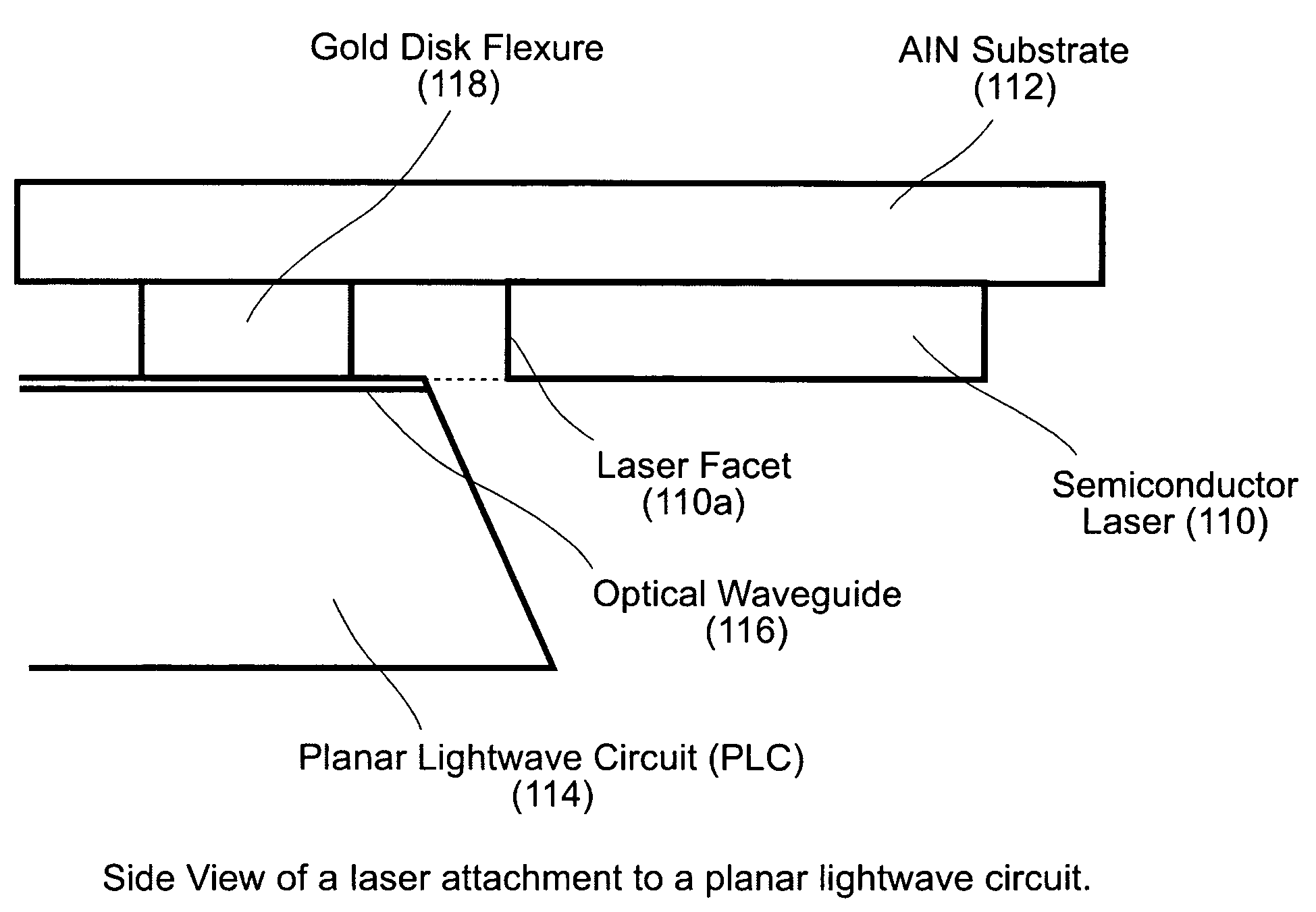
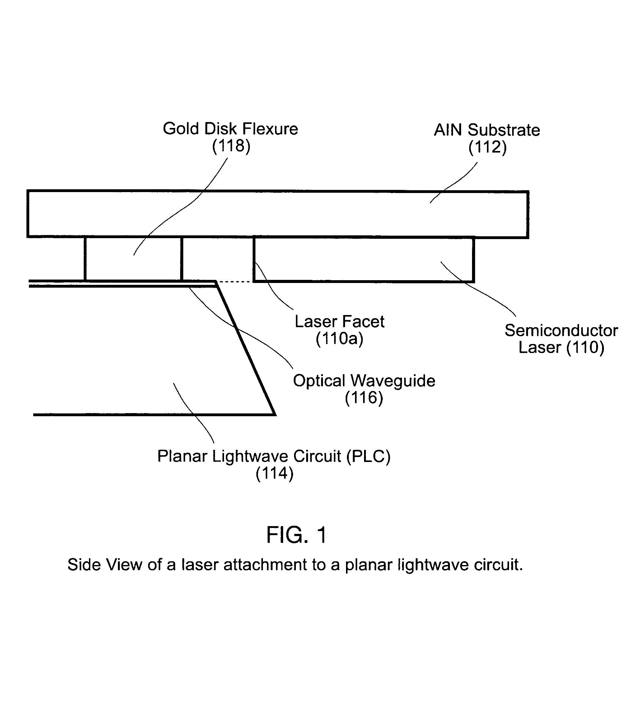
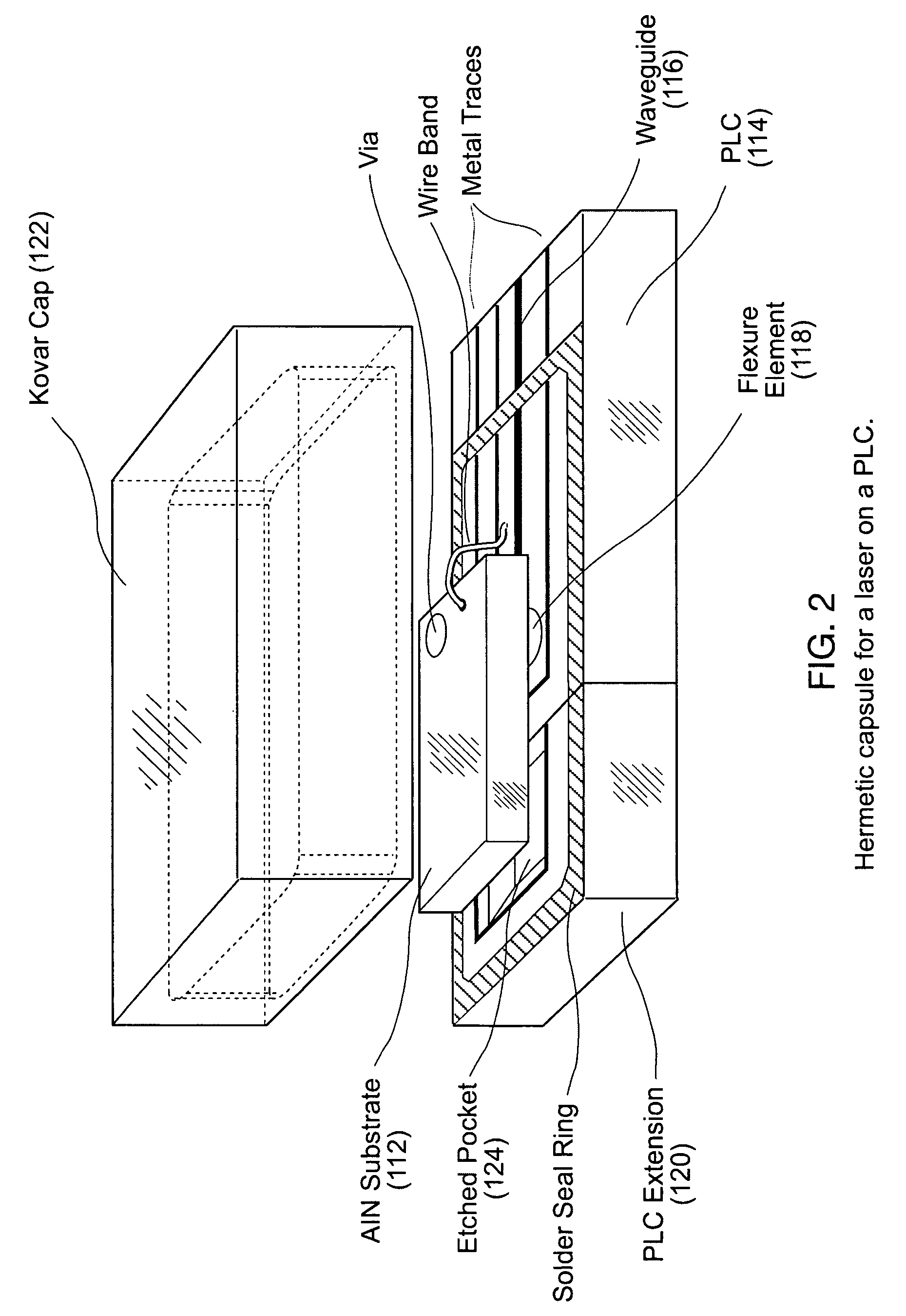
[0037]The present invention attaches and aligns a bulk element such as a semiconductor laser to an optical component formed on a PLC. While the bulk element will be described below for illustrative purposes only as a semiconductor laser, the bulk element alternatively may comprise a variety of different active and / or passive elements that process an optical beam. For example, active devices include semiconductor lasers and amplifiers, light emitting diodes, as well as other devices offering higher levels of functionality. Passive devices include beam splitters, thin films, filters, mirrors, birefringent material, polarizers, and diffractive elements, for example.

[0038]As detailed below, the bulk element is first attached to its own substrate in a conventional manner and the resulting subassembly is bonded to the PLC via a bendable or flexure element of low yield strength that allows for active optical alignment. Active alignment is then achieved by moving the bulk element into its p...


PUM

PropertyMeasurementUnit
diameteraaaaaaaaaa
sizeaaaaaaaaaa
optical coupling efficiencyaaaaaaaaaa

Abstract

A method and apparatus is provided for attaching a bulk element processing an optical beam to a PLC and optically aligning the bulk element with an optical element formed on the PLC. The method begins by securing the bulk element to a first side of a substrate. A first side of a flexure element is secured to the first side of the substrate. A second side of the flexure element is secured to a first side of the PLC on which the optical element is formed such that the bulk element and the optical element are in optical alignment to within a first level of tolerance. Subsequent to the step of securing the second side of the flexure element, a force is exerted on at least a second side of the substrate to thereby flex the flexure element. The force causes sufficient flexure of the flexure element to optically align the bulk element and optical element to within a second level of tolerance that is more stringent than the first level of tolerance.

Description

FIELD OF THE INVENTION[0001]The invention relates generally to fiber optics, and in particular to an arrangement for providing optical alignment between a semiconductor device, such as a laser or detector, and an optical waveguide such as a planar lightwave circuit or an optical fiber.BACKGROUND OF THE INVENTION[0002]In fiber optic technology there are many instances where it is necessary to optically align and optically couple a bulk element such as a semiconductor device and / or a micro electromechanical system (MEMs) to an optical component located on a planar lightwave circuit (PLC). A PLC employs planar optical integration to manufacture waveguide circuits on silicon wafers, using processing techniques similar to those used in the silicon microelectronics industry. Doped-silica waveguides are usually preferred because they have a number of attractive properties including low cost, low loss, stability, and compatibility for coupling to laser diodes, other waveguides, high NA fibe...

Claims


Application Information

Patent Timeline
Patent Type & Authority Patents(United States)
IPC IPC(8): B81C3/00G02B6/26G02B6/36G02B6/42
CPCB81C3/002G02B6/422G02B6/4226G02B6/4238H01L2224/81801H01L2924/01322H01L2924/12041
Inventor BOUDREAU, ROBERT A.
Owner AVAGO TECH INT SALES PTE LTD
Why Eureka
Try Eureka