Method and system for determining repeatable yield detractors of integrated circuits

a technology of repeatable yield and integrated circuit, which is applied in the field of logic system testing, can solve the problems of large determination effort, more difficult diagnosis, and low yield loss relative to the size of the chip, and achieve the effects of reducing the complexity of the process, and improving the reliability of the logic system

Inactive Publication Date: 2005-11-29
INT BUSINESS MASCH CORP
View PDF16 Cites 36 Cited by
  • Summary
  • Abstract
  • Description
  • Claims
  • Application Information

AI Technical Summary

Problems solved by technology

Yield detractors include process random defects, process systematic problems, mask defects or problems, and circuit marginality problems.
Many of these problems have random characteristics, that is, they occur in different areas of the chip and on different circuits without any apparent pattern.
High random defect levels are a serious concern and usually indicate a more systematic problem such as contamination
There are other systematic, or repeatable, yield detractors that are more difficult to diagnose.
These are problems that occur in the logic area of the chip.
They may be caused by circuit marginality, mask defects, or process marginality for structures unique to logic.
If these problems cause very low yield, there is a great effort undertaken to determine the cause and fix the problem.
If the yield loss is low, however, or only occurs on certain lots, it may be interpreted as expected random defects.
“Low” yield loss is relative to the size of the chip, the complexity of the process, and the maturity of the process.
If “expected” yield is 20% and the actual yield is 16%, the difference may be attributed to random defects, when in fact it may be due to systematic defects with a common cause that may be much more easily fixed.
In a test that comprises, for example, 1,000 patterns, if test #512 fails on a number of parts, then repeatable defects are highly suspect.
The existing state of the art has practical limitations.
In practice, much of the chip is tested in the first few patterns so it is natural that earlier patterns will have a higher failure rate and the vast majority of these will not be common fails.
There are still limits to the usefulness of this method, however, because there are on large chips tens or hundreds of thousands of outputs (chip outputs and latches) that are measured.
It is impractical to compare all the possible failure modes for thousands of latches on thousands of patterns across thousands of chips.
Yet one more limitation of the existing method is that it is not applicable to any test that compresses measurements into a register after every cycle.

Method used


Image

  • Method and system for determining repeatable yield detractors of integrated circuits
  • Method and system for determining repeatable yield detractors of integrated circuits
  • Method and system for determining repeatable yield detractors of integrated circuits

Examples


Embodiment Construction

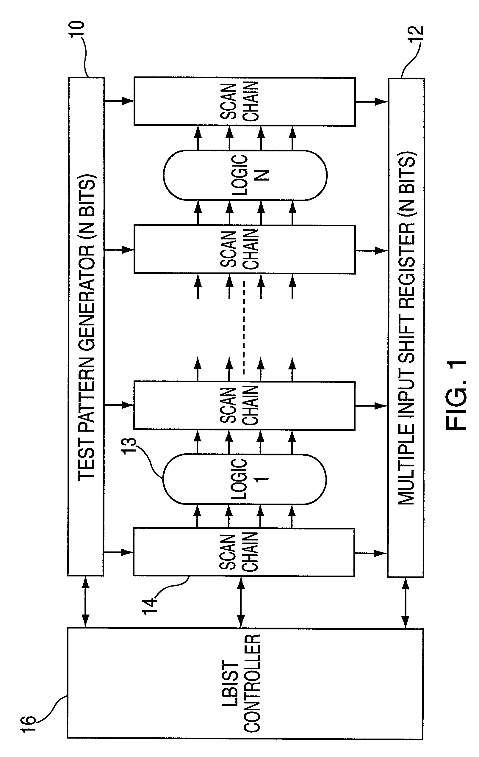
[0021]FIG. 1 shows a high-level overview of the chip LBIST implementation for LBIST testing chip logic with the use of a test pattern generator 10 which is used to generate the test patterns passing through a scan chain 14 to a multiple input signature register (MISR) 12 to compress the test results. An LBIST controller 16 is used to apply the clocks and controls to the test pattern generator, MISR and system logic to perform the test. The test pattern generator 10 of FIG. 1 generates test data which passes through logic via multiple parallel scan chains 14 which are connected between the test pattern generator and MISR 12. The test pattern generator 10 having N bits generates the test data which is scanned into the scan chains 14 as the test pattern for the scan operation portion of the LBIST test of the chip. Clock signals are applied to the logic 13 and the result of the test pattern and logic 13 is scanned out of the scan chains 14 and compressed and stored into the MISR 12 to g...


PUM


Abstract

An exemplary embodiment of the present invention is a method for testing an integrated circuit. The method includes generating a test pattern and generating a reference signature corresponding to the test pattern. An integrated circuit test is executed in response to the test pattern and a result signature is generated in response to data output from executing the integrated circuit test. The result signature is compared to the reference signature and a current failing signature is created if the two don't match. The current failing signature is copy of the result signature. Common error analysis is executed in response to creating the current failing signature. Additional embodiments include a system and storage medium for testing an integrated circuit.

Description

CROSS REFERENCE TO RELATED APPLICATIONS[0001]This is a continuation-in-part of U.S. patent application Ser. No. 09 / 722,880, filed Nov. 27, 2000, now U.S. Pat No. 6,751,765, the entire contents of which are incorporated herein by reference.BACKGROUND OF THE INVENTION[0002]This invention relates to the testing of logic systems in semiconductor integrated circuits or chips. More specifically, the invention relates to a method and apparatus for more easily identifying common causes of logic circuit yield detractors. An alternate embodiment relates to a method and apparatus for more easily identifying common causes of integrated circuit yield detractors.[0003]Yield is the ratio of all good chips to the total number of chips produced. It is an extremely important quantity and often determines if a program is highly profitable or a loss. A major effort in the development of a new semiconductor technology is termed “yield learning.” Yield learning covers all activities to raise yield to vol...

Claims


Application Information

Patent Timeline
Patent Type & Authority Patents(United States)
IPC IPC(8): G01R31/3185
CPCG01R31/3185
Inventor KURTULIK, RAYMOND J.MOTIKA, FRANCORIZZOLO, RICHARD F.
Owner INT BUSINESS MASCH CORP
Why Eureka
Try Eureka