Method for forming dielectric layer between gates in flash memory device

a technology of dielectric layer and flash memory, which is applied in the direction of semiconductor devices, electrical apparatus, transistors, etc., can solve the problems of lowering the yield, and achieve the effect of preventing the variation of the thickness of the dielectric layer

Active Publication Date: 2006-01-10
STMICROELECTRONICS SRL +1
View PDF1 Cites 4 Cited by
  • Summary
  • Abstract
  • Description
  • Claims
  • Application Information

AI Technical Summary

Benefits of technology

[0008]The present invention is directed to a method for forming a dielectric layer between gates in a flash memory device that can prohibit reaction of a floating gate and an oxide film to prevent variation in a thickness of the dielectric layer.

Problems solved by technology

Moreover, since the thickness of the lower oxide film ONO1 is not uniformly increased over the entire wafer, there is a problem that the yield is lowered due to increased dispersion of the threshold voltage at the time of the programming and erasing operations of the device.

Method used


Image

  • Method for forming dielectric layer between gates in flash memory device
  • Method for forming dielectric layer between gates in flash memory device
  • Method for forming dielectric layer between gates in flash memory device

Examples


Embodiment Construction

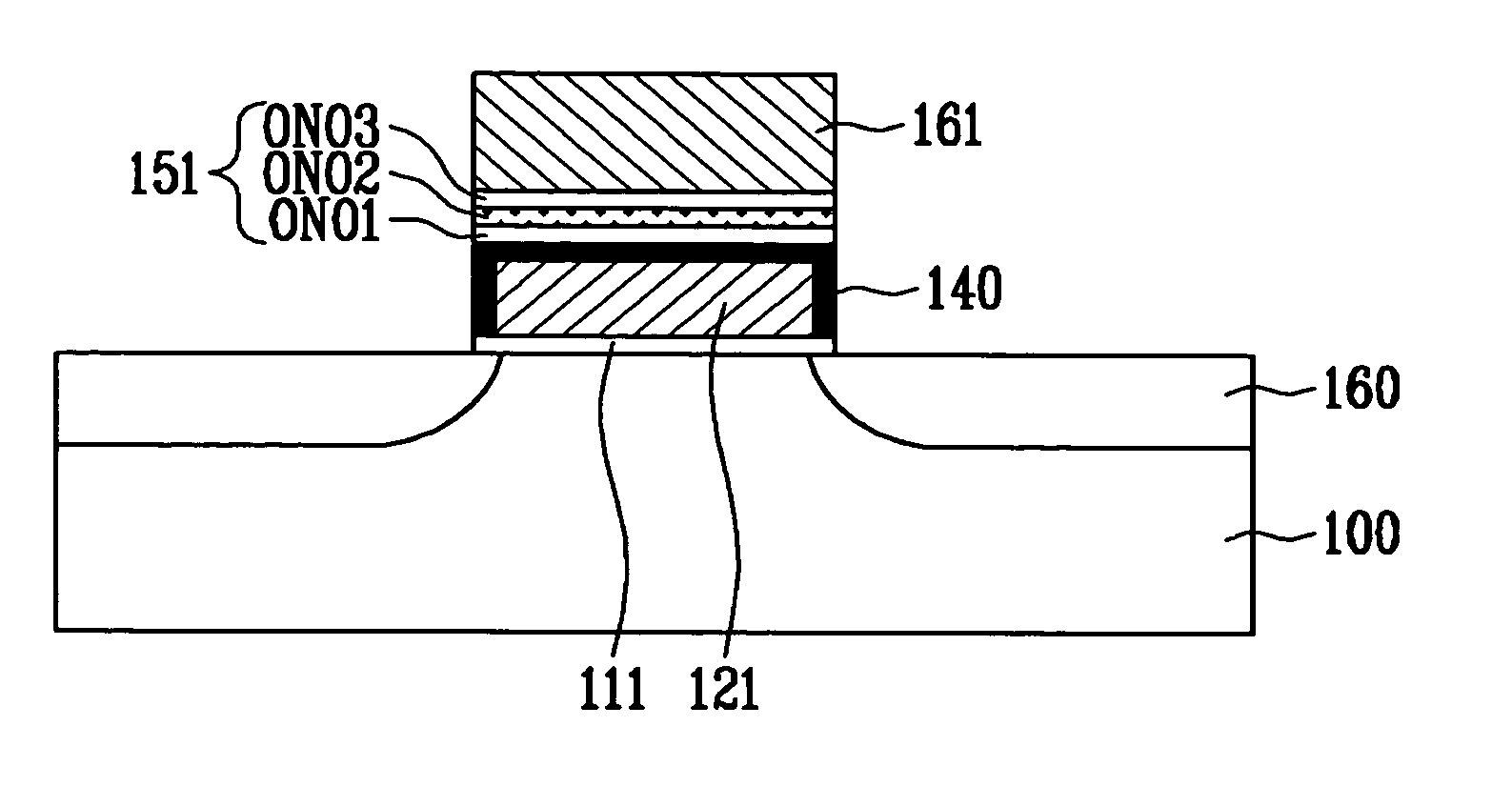
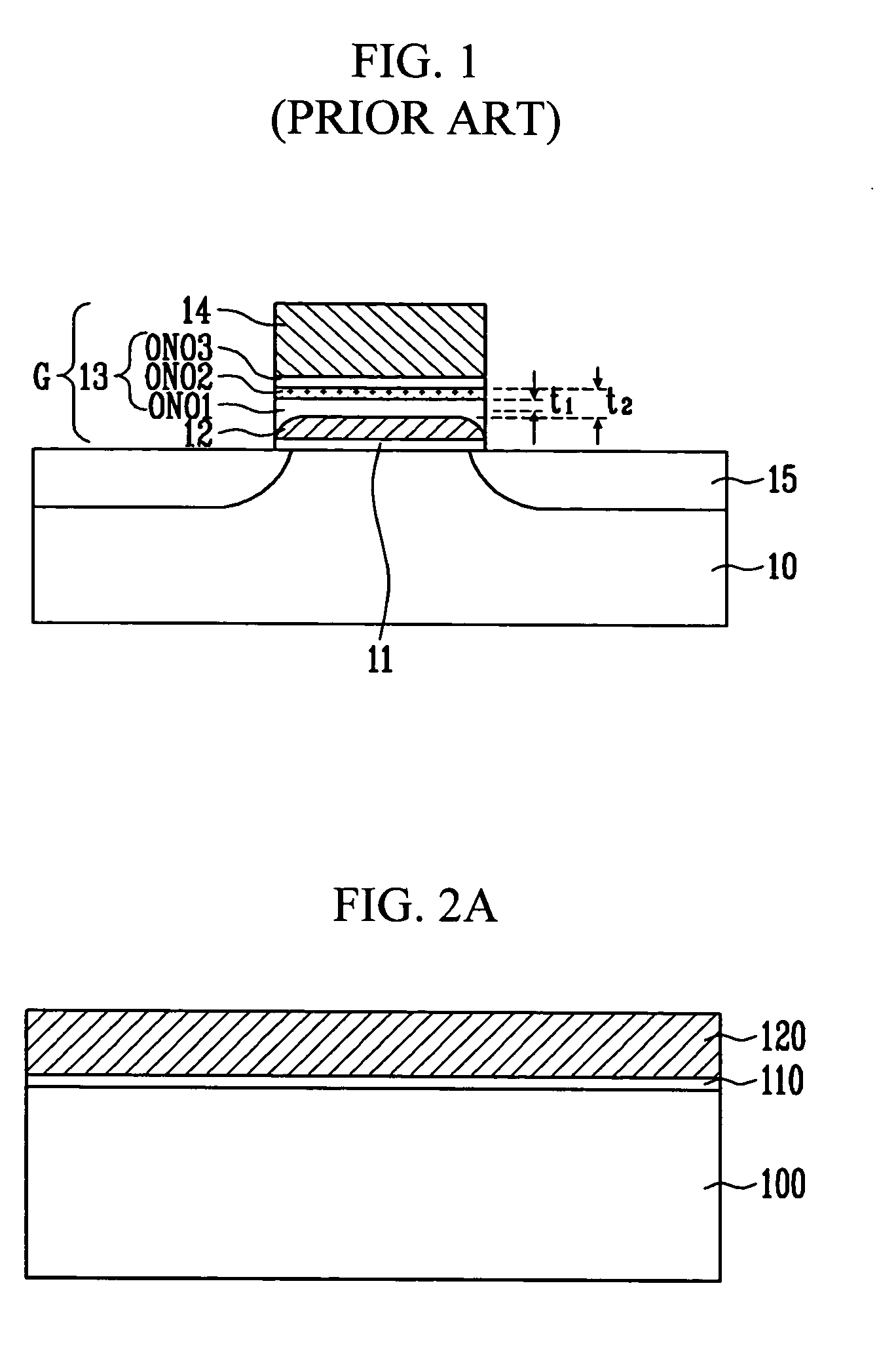
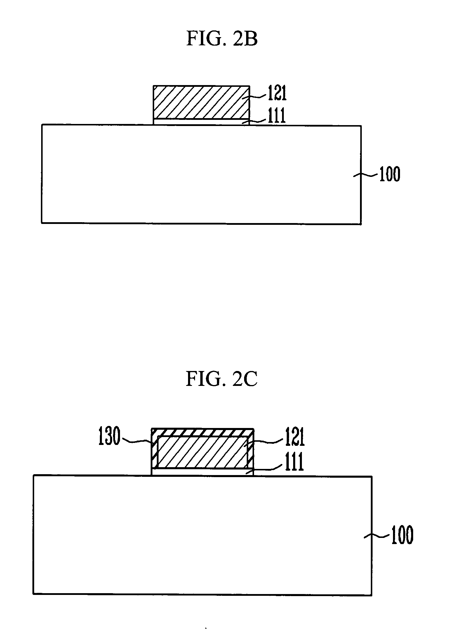
[0016]Now the preferred embodiments according to the present invention will be described with reference to the accompanying drawings. Since preferred embodiments are provided for the purpose that the ordinary skilled in the art are able to understand the present invention, they may be modified in various manners and the scope of the present invention is not limited by the preferred embodiments described later. Further, in the drawing, the thickness and size of each layer are exaggerated for convenience of explanation and clarity. Like reference numerals are used to identify the same or similar parts. Meanwhile, in case where it is described that one film is “on” the other film or a semiconductor substrate, the one film may directly contact the other film or the semiconductor substrate. Or, a third film may be intervened between the one film and the other film or the semiconductor substrate.

[0017]A method for manufacturing a flash memory device according to an embodiment of the prese...


PUM

PropertyMeasurementUnit
temperatureaaaaaaaaaa
pressureaaaaaaaaaa
temperatureaaaaaaaaaa

Abstract

The present invention provides a method for preventing an oxide film from becoming thick due to the reaction of the oxide film and a floating gate in a method for manufacturing a flash memory device having a dielectric layer consisting of at least one oxide film between the floating gate and a control gate. To this end, a Si—F bonding layer is formed on the surface of a silicon film constituting the floating gate. The Si—F bonding layer is annealed in a nitrogen gas atmosphere to form a Si—N bonding layer. A dielectric layer is then formed.

Description

BACKGROUND[0001]1. Field of the Invention[0002]The present invention relates to a method for manufacturing a flash memory device, and more specifically, to a method for forming a dielectric layer between gates in a flash memory device.[0003]2. Discussion of Related Art[0004]Programming and erasing operations in a flash memory device are accomplished by storing or erasing charges in or from a floating gate. The programming and erasing properties are dependent on the coupling ratio between the floating gate and the control gate. It is thus necessary to form a dielectric layer between the floating gate and the control gate in a uniform thickness.[0005]A conventional method for manufacturing a flash memory device will be described with reference to FIG. 1.[0006]A gate pattern G consisting of a tunnel oxide film 11, a floating gate 12, an ONO dielectric layer 13 and a control gate 14 is formed on a semiconductor substrate 10. An impurity is doped into the semiconductor substrate 10 to fo...

Claims


Application Information

Patent Timeline
Patent Type & Authority Patents(United States)
IPC IPC(8): H01L21/336H01L21/318H01L21/8247H01L27/115H01L29/788H01L29/792H01L29/94
CPCH01L29/7883H01L29/792H01L21/823437
Inventor PARK, SANG WOOK
Owner STMICROELECTRONICS SRL
Why Eureka
Try Eureka