Integrated circuit devices including input/output line pairs and precharge circuits and related memory devices

a technology of integrated circuits and memory devices, which is applied in the direction of information storage, static storage, digital storage, etc., can solve the problems of pre-charge circuits, regions may not be able to charge gio with sufficient speed, and cannot pre-charge or equalize gio in a given period of tim

Inactive Publication Date: 2006-01-10
SAMSUNG ELECTRONICS CO LTD
View PDF7 Cites 384 Cited by
  • Summary
  • Abstract
  • Description
  • Claims
  • Application Information

AI Technical Summary

Benefits of technology

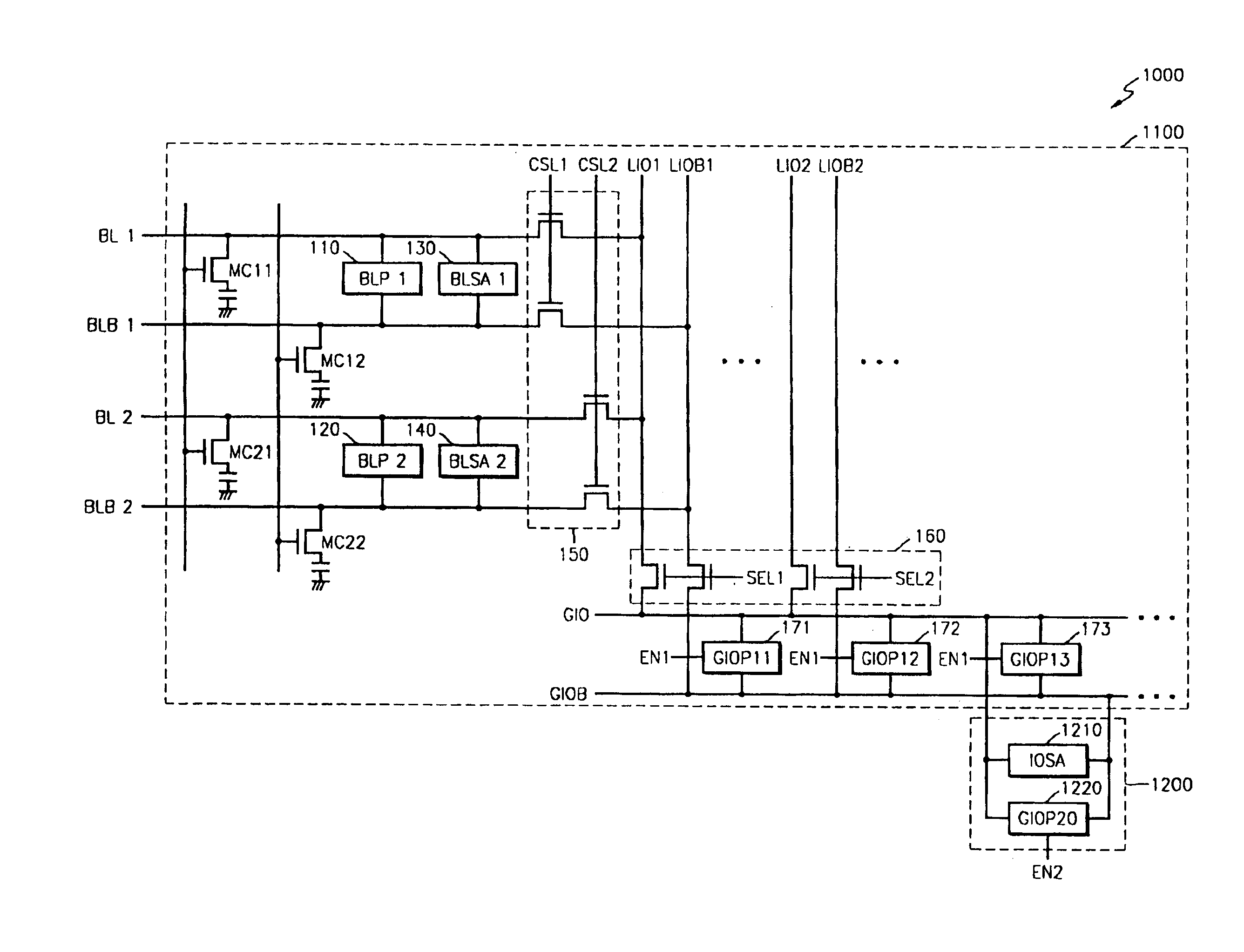
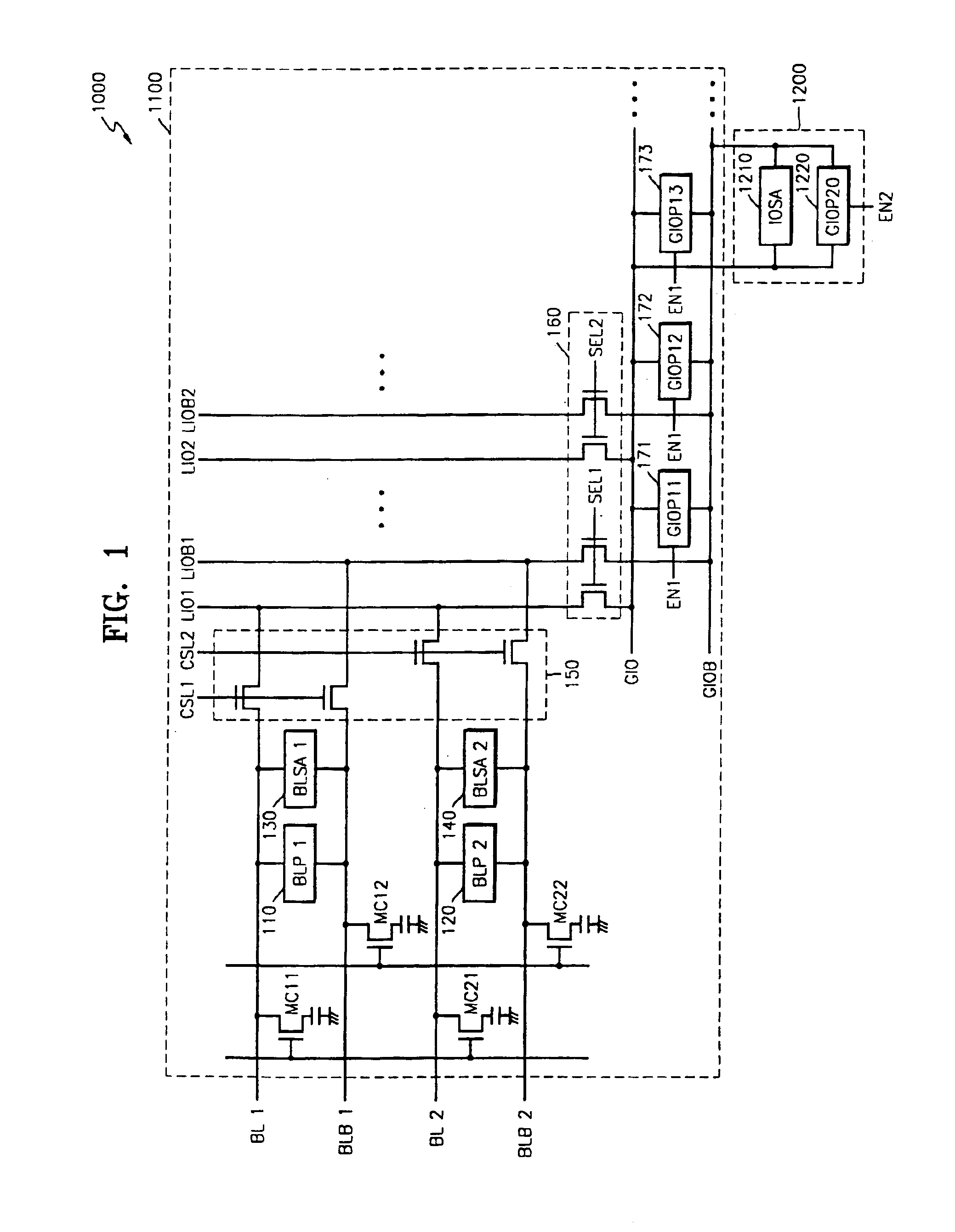
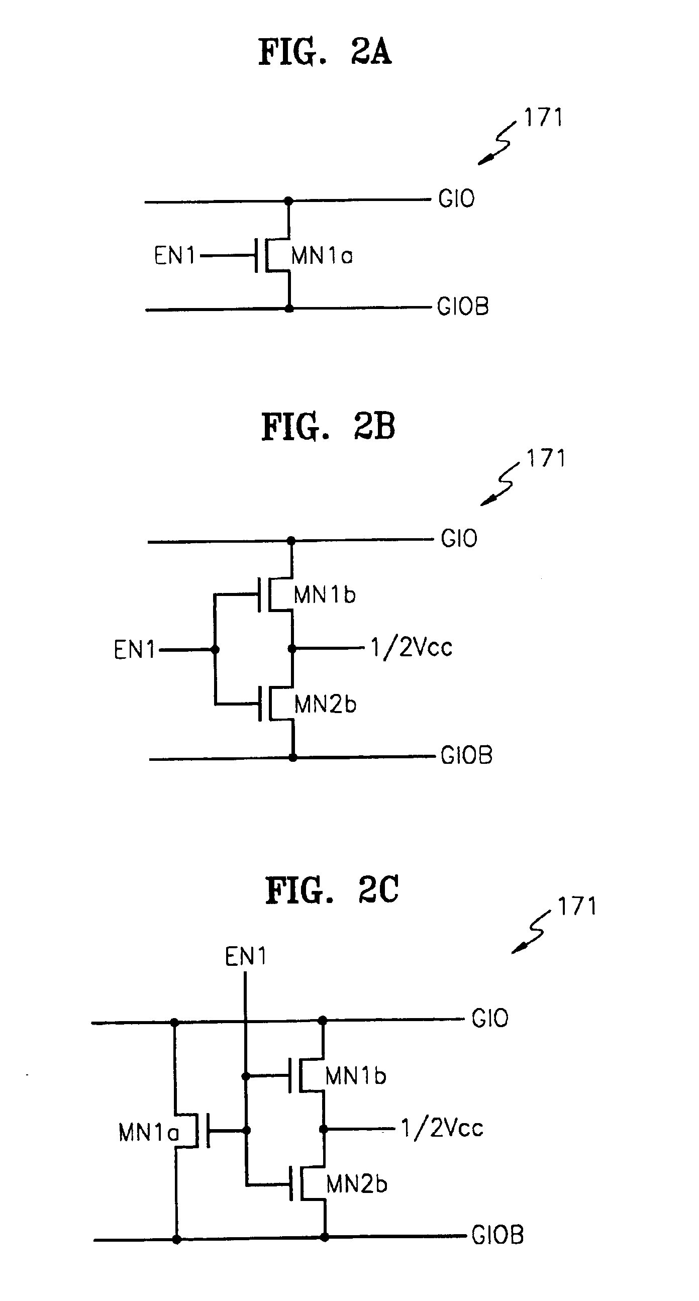
[0015]More particularly, the precharge circuit may include a transistor having a first source / drain region connected to the first input / output line, a second source / drain region connected to the second input / output line, and a control electrode between the first and second source / drain regions. The transistor may electrically connect the first and second input / output lines responsive to the enable signal being applied to the gate electrode. Moreover, the transistor may be a metal-oxide-semiconductor MOS transistor.
[0016]In addition or in an alternative, the precharge circuit may include first and second serially connected transistors. The first transistor may have a first source / drain region connected to the first input / output line, a second source / drain region connected to a voltage source, and a control electrode between the first and second source / drain regions. The second transistor may have a third source / drain region connected to the second input / output line, a fourth source / drain region connected to the voltage source, and a control electrode between the third and fourth source / drain regions. Moreover, the voltage source may be electrically connected to the first and second input / output lines responsive to the enable signal being applied to the control electrodes of the first and second transistors. In addition, the voltage source may provide a voltage of approximately ½ of a power supply voltage for the integrated circuit device, and the first and second transistors may include first and second metal-oxide-semiconductor MOS transistors.

Problems solved by technology

If the distance is too great, a precharge circuit in the peripheral region may be unable to charge the GIO with sufficient speed.
Thus, the precharge circuit of the GIO, positioned at the peripheral region, may not precharge or equalize the GIO in a given period of time.
Therefore, the precharge circuit of the GIO, positioned at the peripheral region, may not be able to precharge the IO line in a given period of time allowed at a higher operating speed.
If the IO line is not precharged in a given period of time allowed for a particular specification, operation errors may occur when data is written to or read from a memory.

Method used


Image

  • Integrated circuit devices including input/output line pairs and precharge circuits and related memory devices
  • Integrated circuit devices including input/output line pairs and precharge circuits and related memory devices
  • Integrated circuit devices including input/output line pairs and precharge circuits and related memory devices

Examples


Embodiment Construction

[0024]The present invention will be described more fully hereinafter with reference to the accompanying drawings, in which typical embodiments of the invention are shown. This invention, however, may be embodied in many different forms and should not be construed as limited to the embodiments set forth herein. Rather, these embodiments are provided so that this disclosure will be thorough and complete, and will fully convey the scope of the invention to those skilled in the art. It will also be understood that when an element is referred to as being “coupled” or “connected” to another element, it can be directly coupled or connected to the other element or intervening elements may also be present. In contrast, when an element is referred to as being “directly coupled” or “directly connected” to another element, there are no intervening elements present. Like numbers refer to like elements throughout.

[0025]FIG. 1 illustrates a semiconductor device including a precharge circuit accord...


PUM


Abstract

An integrated circuit device may include a pair of first and second input/output lines on a substrate and a precharge circuit connected to the first and second input/output lines. More particularly, portions of the first and second input/output lines may extend in a parallel direction along first lengths thereof, portions of the first and second input/output lines may cross one another in a twist region so that portions of the first and second input/output lines in the twist region extend in directions different than the parallel direction, and portions of the first and second input/output lines may extend in the parallel direction along second lengths. Accordingly, relative positions of the first and second input/output lines may be reversed in the first and second lengths thereof. In addition, the precharge circuit may be connected to portions of the first and second input/output lines in the twist region extending in the directions different than the parallel direction, and the precharge circuit may be configured to provide that the first and second input/output lines have a same electrical potential responsive to an enable signal. Related memory devices are also discussed.

Description

RELATED APPLICATIONS[0001]This application claims the benefit of priority from Korean Patent Application No. 2002-77035 filed on Dec. 5, 2002, in the Korean Intellectual Property Office, the disclosure of which is incorporated herein in its entirety by reference.FIELD OF THE INVENTION[0002]The present invention relates to integrated circuit devices, and more particularly, to integrated circuit devices with input / output line pairs and related memory devices.BACKGROUND OF THE INVENTION[0003]In semiconductor devices, various input / output lines (IO lines) may be used to read data from a memory cell or write data to a memory cell. Since a pair of IO lines may have different voltage levels after an IO line performs a write command or a read command, the IO line may be precharged before performing a next command.[0004]An IO line of a semiconductor device may include a first IO line coupled to a bit line coupled to a memory cell via a column select circuit, and a second IO line coupled to t...

Claims


Application Information

Patent Timeline
Patent Type & Authority Patents(United States)
IPC IPC(8): G11C7/00G11C7/12G11C11/4094G11C11/4097
CPCG11C7/12G11C11/4097G11C11/4094
Inventor KIM, SUNG-HOON
Owner SAMSUNG ELECTRONICS CO LTD
Why Eureka
Try Eureka