Data storage devices with wafer alignment compensation

a data storage device and wafer technology, applied in the field of data storage devices, can solve the problems of inability of the data storage device to write data to and/or read data from one or more storage areas, and one or more of the emitters of the second wafer may not be appropriately aligned with respect to the corresponding storage area of the first wafer

Inactive Publication Date: 2006-01-17
SAMSUNG ELECTRONICS CO LTD
View PDF2 Cites 17 Cited by
  • Summary
  • Abstract
  • Description
  • Claims
  • Application Information

AI Technical Summary

Problems solved by technology

Due to various fabrication tolerances, however, one or more of the emitters of the second wafer may not be appropriately aligned with respect to corresponding storage areas of the first wafer.
This misalignment could potentially result in an inability of the data storage device to properly write data to and / or read data from one or more of the storage areas.

Method used


Image

  • Data storage devices with wafer alignment compensation
  • Data storage devices with wafer alignment compensation
  • Data storage devices with wafer alignment compensation

Examples


Embodiment Construction

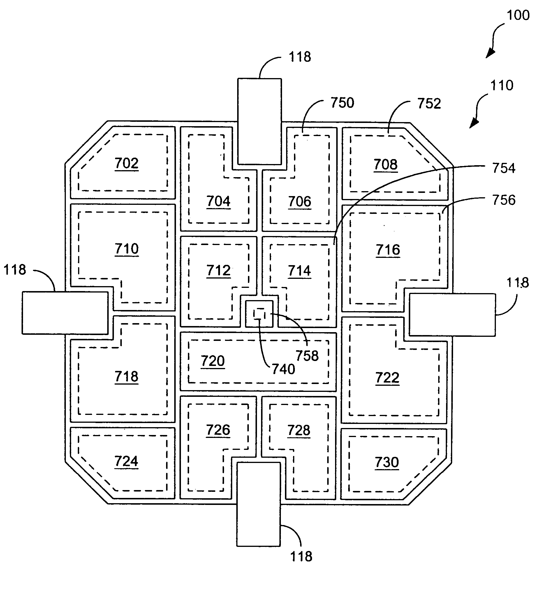
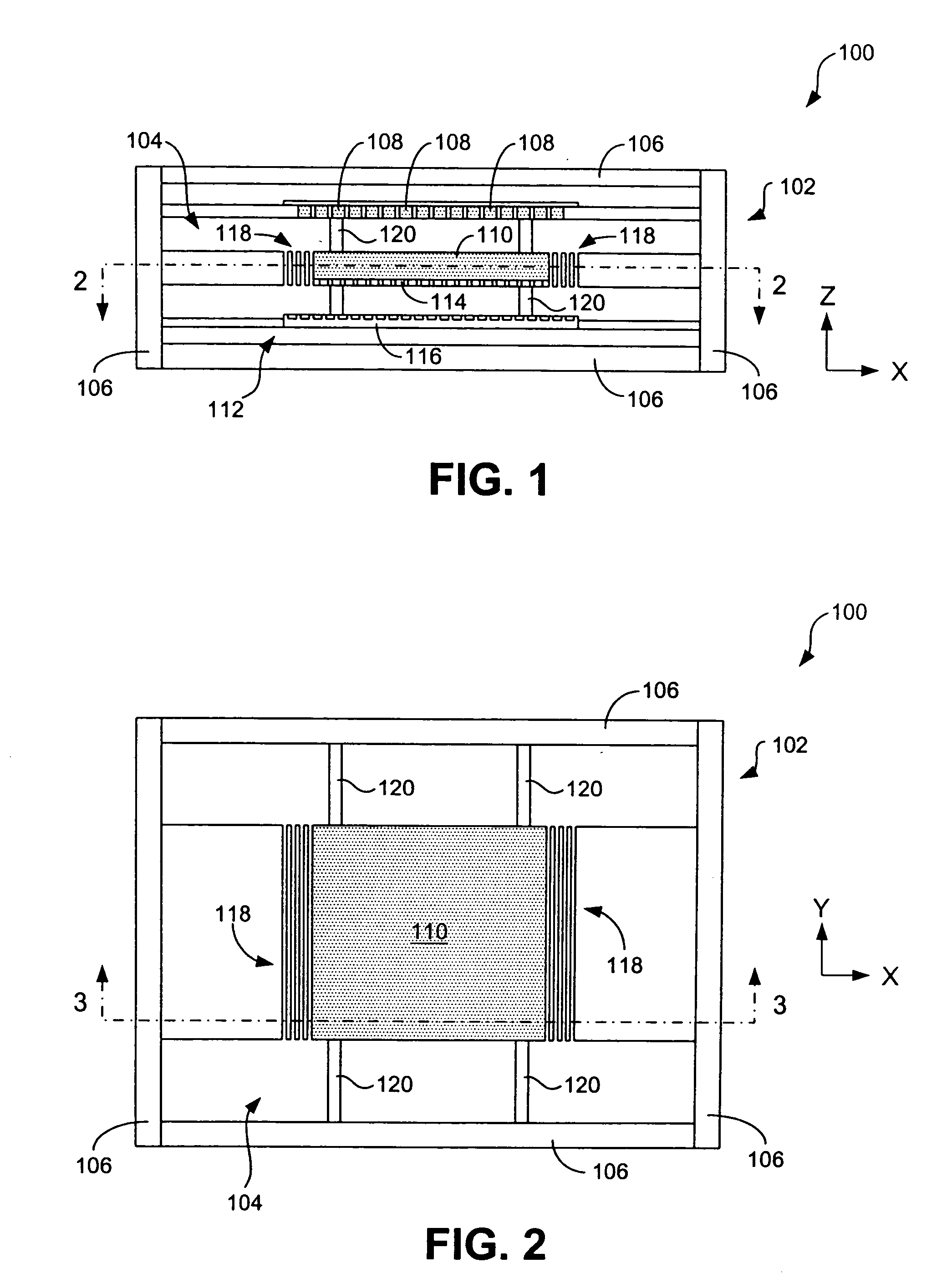
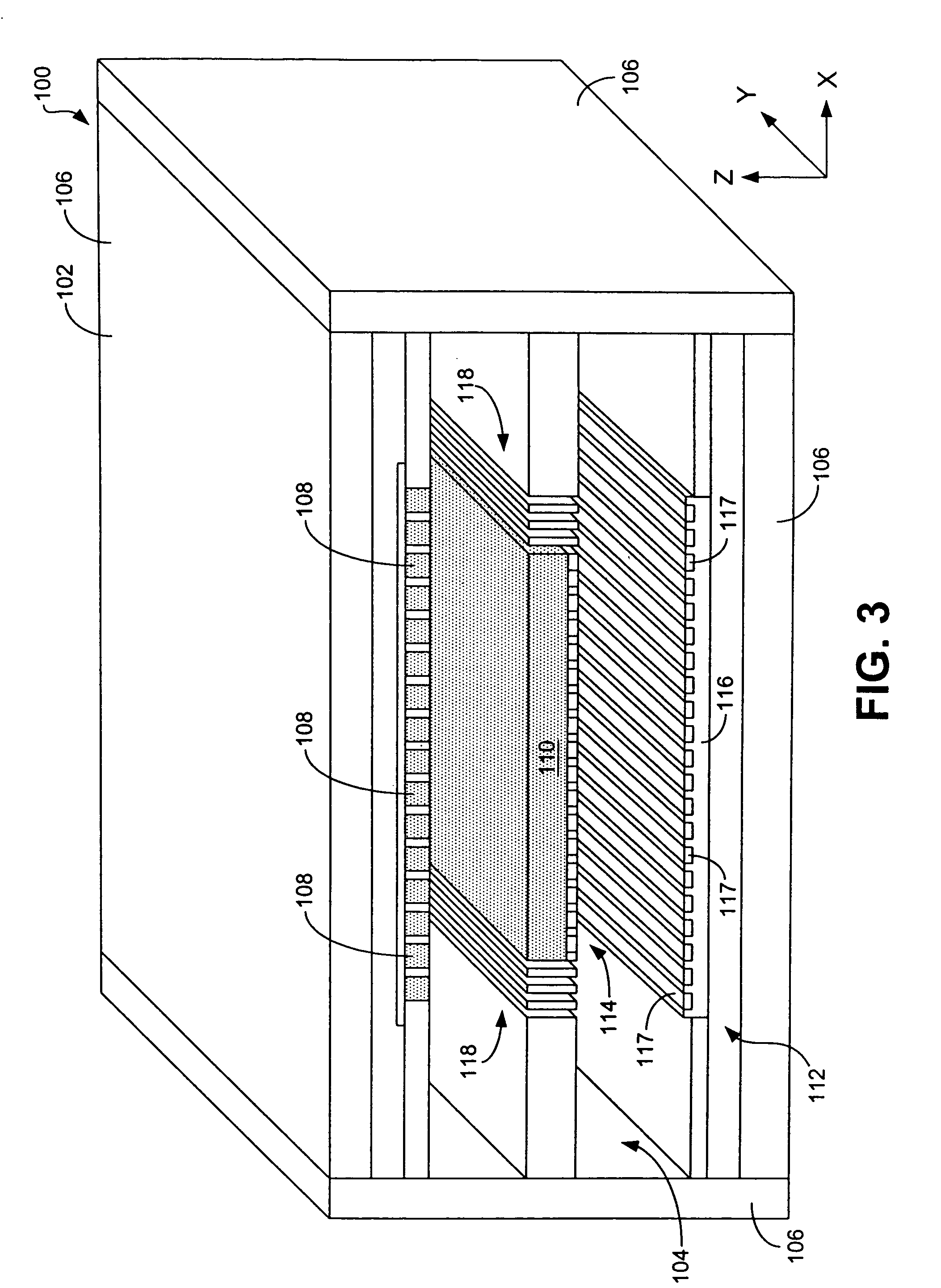
[0024]Referring now in more detail to the drawings, in which like numerals indicate corresponding parts throughout the several views, FIGS. 1–3 illustrate a representative data storage device 100. It is noted that data storage device 100 is similar in construction to that described in U.S. Pat. No. 5,557,596, which is incorporated by reference herein.

[0025]As indicated in FIGS. 1–3, data storage device 100 generally includes an outer casing 102 that defines an interior space 104. By way of example, the casing 102 can include walls 106 that define the interior space. Typically, walls 106 are sealed to each other so that a vacuum can be maintained within the interior space. For instance, a vacuum of at least approximately 10–3 Torr is maintained within the interior space in some embodiments. Although a particular configuration is shown for the casing 102, it is to be understood that the casing can take many different forms that would be readily apparent to persons having ordinary skil...


PUM

PropertyMeasurementUnit
widthaaaaaaaaaa
storage areaaaaaaaaaaa
areaaaaaaaaaaa

Abstract

Methods for storing data are provided. Preferably, the method includes the steps of: providing a data storage device, and preventing an emitter associated with a first data cluster of the data storage device from writing data to another one of the data clusters. Data storage devices also are provided.

Description

CROSS REFERENCE TO RELATED APPLICATIONS[0001]This application is a continuation application, which is based on and claims priority to U.S. Utility patent application Ser. No. 09 / 910,530, filed on Jul. 20, 2001, now U.S. Pat. No. 6,700,853, and which is incorporated herein in its entirety.BACKGROUND OF THE INVENTION[0002]1. Field of the Invention[0003]The present invention relates to data storage devices and, in particular, to systems and methods utilizing atomic resolution storage techniques for storing data.[0004]2. Background of the Invention[0005]Recently developed semiconductor-based electron sources can be used in data storage devices, such as hard drives, optical drives, and dynamic random access memory (DRAM), for example. An example of such a data storage device is described in U.S. Pat. No. 5,557,596. The device described in that patent includes multiple electron emitters with electron emission surfaces that face a storage medium. During write operations, the electron sourc...

Claims


Application Information

Patent Timeline
Patent Type & Authority Patents(United States)
IPC IPC(8): G11B9/10G11B9/00
CPCB82Y10/00G11B9/1418G11B9/14G11B9/10
Inventor RAESE, J. CRAIG
Owner SAMSUNG ELECTRONICS CO LTD
Why Eureka
Try Eureka