
Defect detection using multiple sensors and parallel processing

a technology of parallel processing and defect detection, applied in the direction of instruments, electric controllers, image enhancement, etc., can solve the problems of defect detection between any two device areas, affecting the yield of devices, and affecting the quality of semiconductor materials,

Active Publication Date: 2006-01-24
KLA TENCOR TECH CORP
View PDF14 Cites 33 Cited by
  • Summary
  • Abstract
  • Description
  • Claims
  • Application Information

AI Technical Summary

Problems solved by technology

Generally, the industry of semiconductor manufacturing involves highly complex techniques for integrating circuits into semiconductor materials.
Due to the large number of processing steps and the decreasing size of semiconductor devices, the semiconductor manufacturing process is prone to processing defects that decrease device yields.
Since many, if not all, of the device areas are identical to each other, any differences detected between any two of the device areas can be a defect.

Method used


Image

  • Defect detection using multiple sensors and parallel processing
  • Defect detection using multiple sensors and parallel processing
  • Defect detection using multiple sensors and parallel processing

Examples


Embodiment Construction

[0024]The present invention will now be described in detail with reference to a few preferred embodiments thereof as illustrated in the accompanying drawings. In the following description, numerous specific details are set forth in order to provide a thorough understanding of the present invention. It will be apparent, however, to one skilled in the art, that the present invention can be practiced without some or all of these specific details. In other instances, well known operations have not been described in detail so not to unnecessarily obscure the present invention.

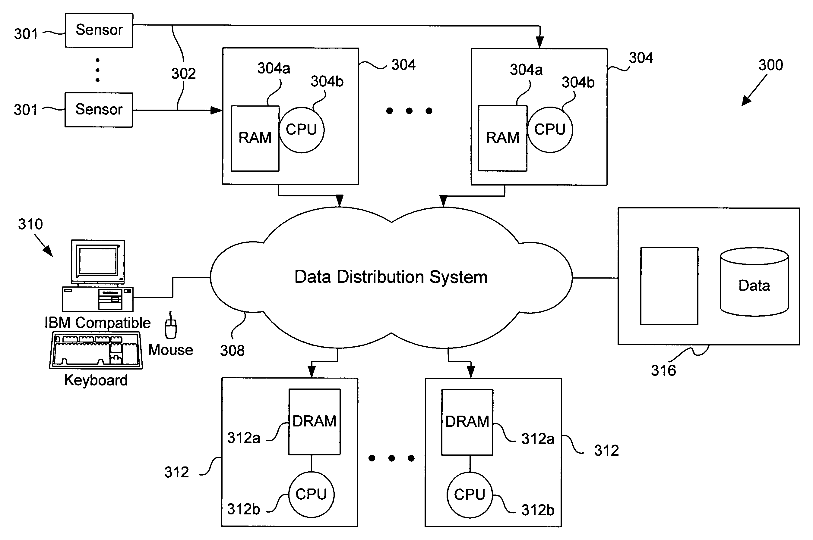
[0025]FIG. 1 is a diagrammatic representation of an inspection system 300 in accordance with one embodiment of the present invention. The inspection system includes input data 302 from a set of sensors 301, optional memory devices 304, a data distribution system 308, a group of processing nodes 312, an optional mass storage device 316, and a system control processor 310. A processing node typically can include one o...


PUM


Abstract

Techniques for detecting defects on semiconductor wafers are described. The techniques involve a parallel processing system wherein a data distribution system contains data distribution nodes that are interconnected by multiple data transfer paths. This configuration allows data collected by any of the detectors to be routed to any one of a plurality of processing nodes. This in turn allows a variety of defect analysis algorithms to be implemented.

Description

CROSS-REFERENCE TO RELATED APPLICATIONS[0001]This application claims priority of U.S. provisional patent application No. 60 / 444,754, filed Feb. 3, 2003, entitled “DEFECT DETECTION USING MULTIPLE SENSORS AND PARALLEL PROCESSING,” which is hereby incorporated by reference.[0002]This application is related to U.S. patent application No. 60 / 132,872, filed May 5, 1999, entitled “Method and Apparatus for Inspecting Reticles Implementing Parallel Processing”, the content of which is hereby incorporated by reference.FIELD OF THE INVENTION[0003]The present invention relates generally to semiconductor wafer inspection, and more specifically to parallel processing techniques for semiconductor wafer inspection.BACKGROUND OF THE INVENTION[0004]Generally, the industry of semiconductor manufacturing involves highly complex techniques for integrating circuits into semiconductor materials. Due to the large number of processing steps and the decreasing size of semiconductor devices, the semiconductor...

Claims


Application Information

Patent Timeline
Patent Type & Authority Patents(United States)
IPC IPC(8): G06F19/00G05B11/01G06F15/16G01R31/26
CPCG01R31/31717G06T7/001G01R31/2834G06T2207/30148G06T2207/10061
Inventor SMITHJOHNSON, ERIK
Owner KLA TENCOR TECH CORP
Learn More