Compliant surface mount electrical contacts for circuit boards and method of making and using same

a surface mount and circuit board technology, applied in the field of electrical contacts, can solve the problems of uneven deformation, broken contacts and/or contacts, and relatively small bonds that cannot resist much mechanical stress, so as to reduce mechanical stress, and avoid excessive lateral expansion

Inactive Publication Date: 2006-02-14
ZIERICK MFG
View PDF7 Cites 93 Cited by
  • Summary
  • Abstract
  • Description
  • Claims
  • Application Information

AI Technical Summary

Benefits of technology

[0010]It is an object of the present invention to provide an electrical contact that is deformable, compliant, and / or flexible to alleviate mechanical stress created by relative movement of printed circuit boards and / or off-board components interconnected by the electrical contact.
[0011]It is also an object of the present invention to provide a pin-type electrical contact having at least one deformable segment along the length thereof that may alleviate stress created by relative movement of printed circuit boards and / or off-board components interconnected by the electrical contact.
[0012]It is another object of the present invention to provide such a pin-type electrical contact that has a symmetrical or otherwise balanced configuration to provide even expansion and avoid excessive lateral expansion.
[0013]It is a further object of the present invention to provide an electrical contact that stops or breaks the capillary flow of solder therein, so as to control the amount of solder that is wicked up from the conductive land into the electrical contact.
[0014]These and other objects of the present invention are accomplished by an electrical contact having a base section and a pin section, which extends from the base section at an angle substantially perpendicular to the base section. The pin section comprises two overlapping legs that are joined at a tip. Each leg has a deformable segment or segments that can expand or contract along the direction of the leg to alleviate stress created by relative movement of printed circuit boards and / or off-board components interconnected by the electrical contact. The deformable segments have members that project or extend in opposing directions relative to an axis of the pin section, so that the segments are symmetrical or otherwise balanced, which prevents the segments from twisting and / or expanding unevenly. In one embodiment of the present invention, each leg has a deformable segment having a outwardly curved or “C” shape. In another embodiment of the present invention, each leg has a deformable segment in the shape of a rectangular frame. The rectangular frames allow the electrical contact to withstand mechanical stresses normally experienced between interconnected printed circuit boards due to the possibility of deflection or deformation of the transverse portions of the rectangular frames. Moreover, due to their configurations, the deformable segments define at least one opening where the two legs of the pin section are not overlapping, which stops or breaks the capillary flow of solder between the legs when the electrical contact is soldered to a conductive land on a PCB. The amount of solder that flows into the electrical contact is selectively controlled or limited by the selected placement of the deformable segments.

Problems solved by technology

Unfortunately, these rigid, relatively small bonds are not able to resist much mechanical stress.
Thus, relative movement of connected PCBs, for example, due to thermal expansion, often results in broken bonds and / or contacts.
However, these previously described compliant electrical contacts do not have at least one deformable section that is symmetrical or otherwise balanced about the centerline thereof and, thus, are prone to uneven deformation and excessive lateral flexibility.
However, if too much solder is wicked away from the conductive land, the bond between the conductive land and the electrical contact is weakened.
Excessive capillary flow of solder is especially troublesome for pin contacts, which often have small bases and long pin sections that wick a relatively large amount of solder from the conductive land.

Method used


Image

  • Compliant surface mount electrical contacts for circuit boards and method of making and using same
  • Compliant surface mount electrical contacts for circuit boards and method of making and using same
  • Compliant surface mount electrical contacts for circuit boards and method of making and using same

Examples


second embodiment

[0042]Referring to FIGS. 8 and 9, an electrical contact according to the present invention is illustrated thereby and indicated generally as 800. Like electrical contact 100, electrical contact 800 has a base 810, a first pin segment or leg 820, and a second pin segment or leg 830.

[0043]First and second pin legs 820 and 830 extend vertically from base 810 at an angle substantially perpendicular to base 810. First pin leg 820 has a first deformable section 825, while second pin leg 830 has a second deformable section 835. First pin leg 820 and second pin leg 830 are connected at an intermediate portion 840, which defines the tip of electrical contact 800. Preferably, intermediate portion 840 is narrowed or necked down compared to pin legs 820 and 830.

[0044]The shape of both deformable sections 825 and 835 is exemplified by reference specifically to first deformable section 825. First deformable section 825 is curved out of alignment with first pin leg 820. Deformable section 825 will...

first embodiment

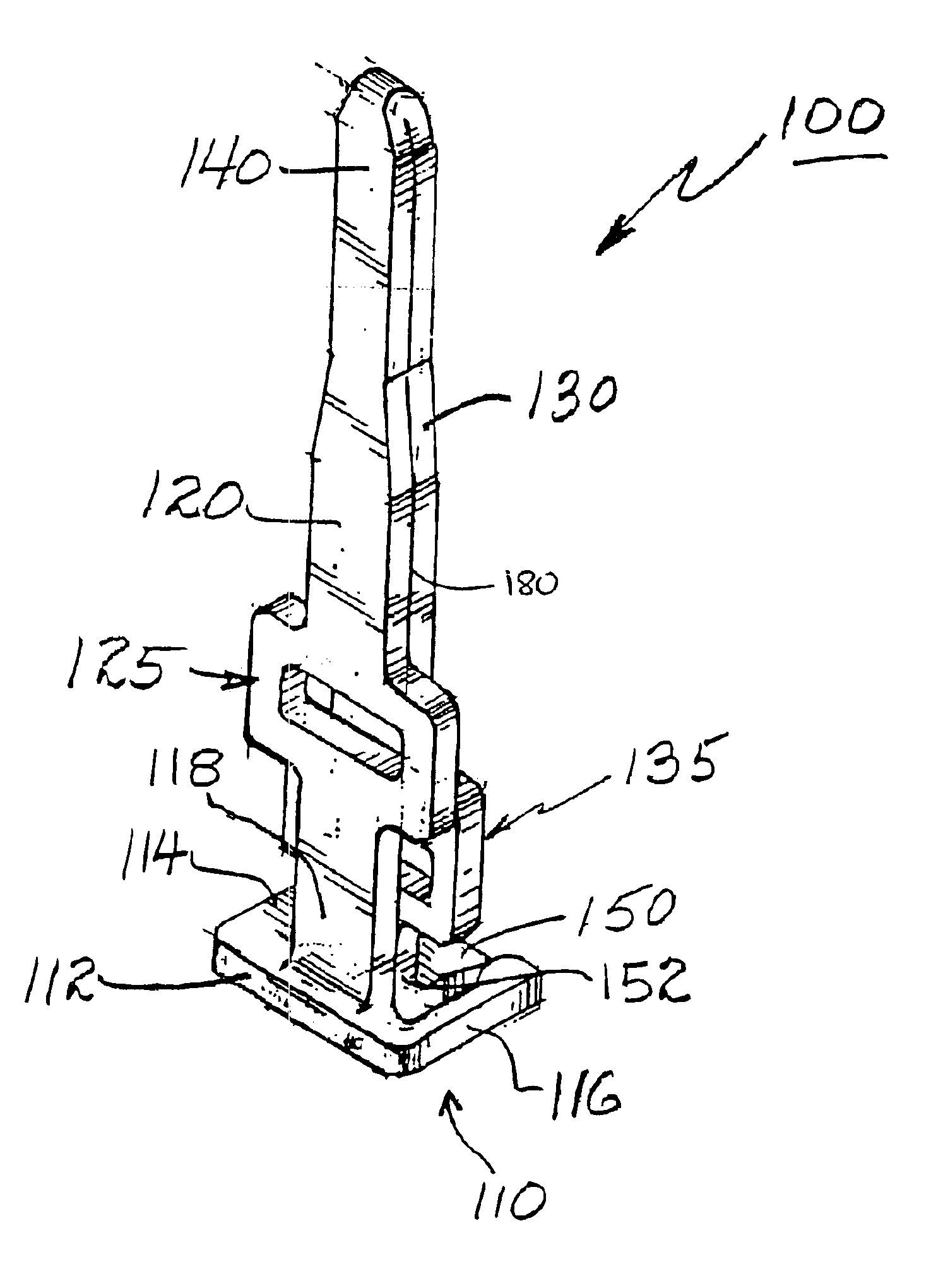
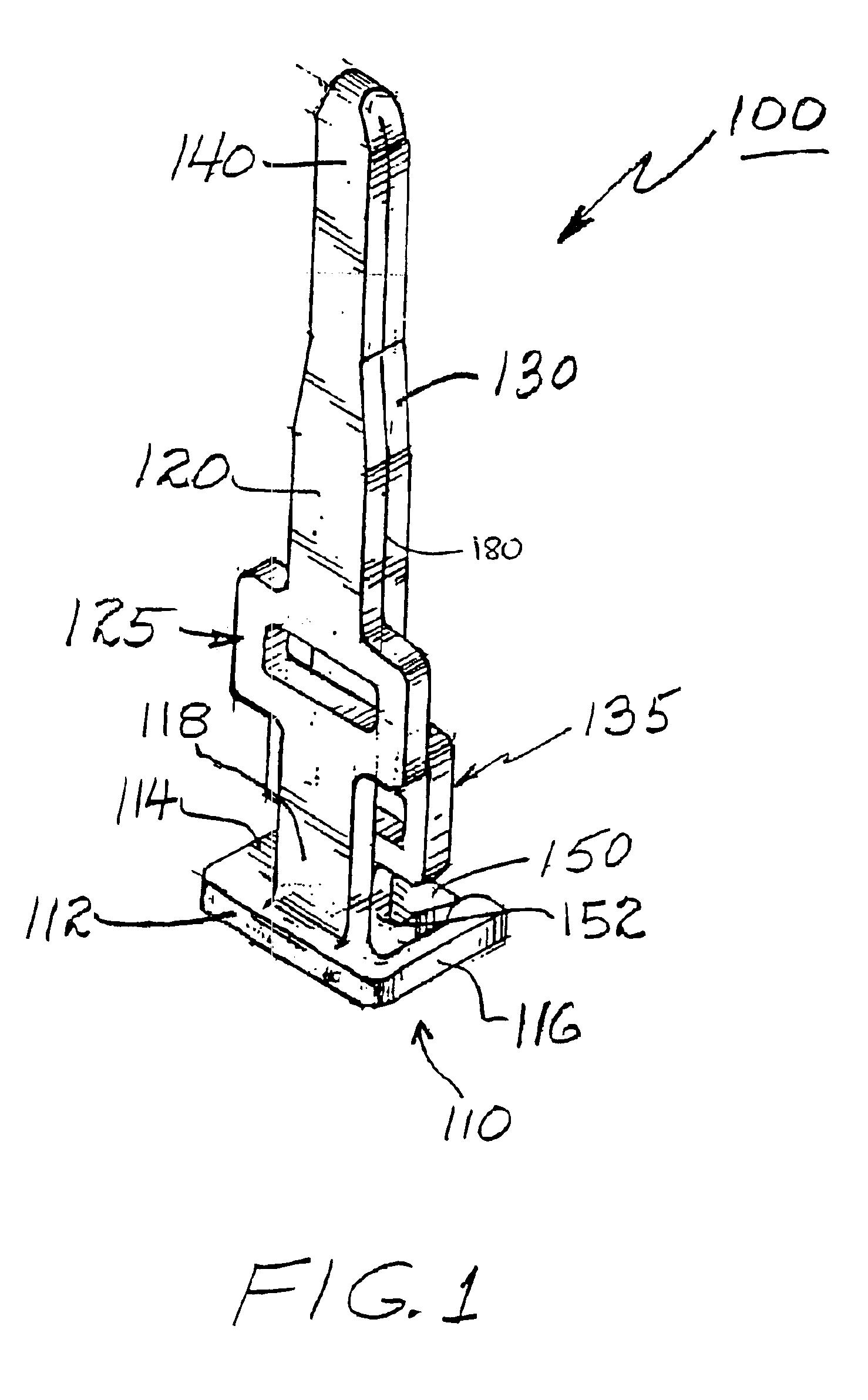
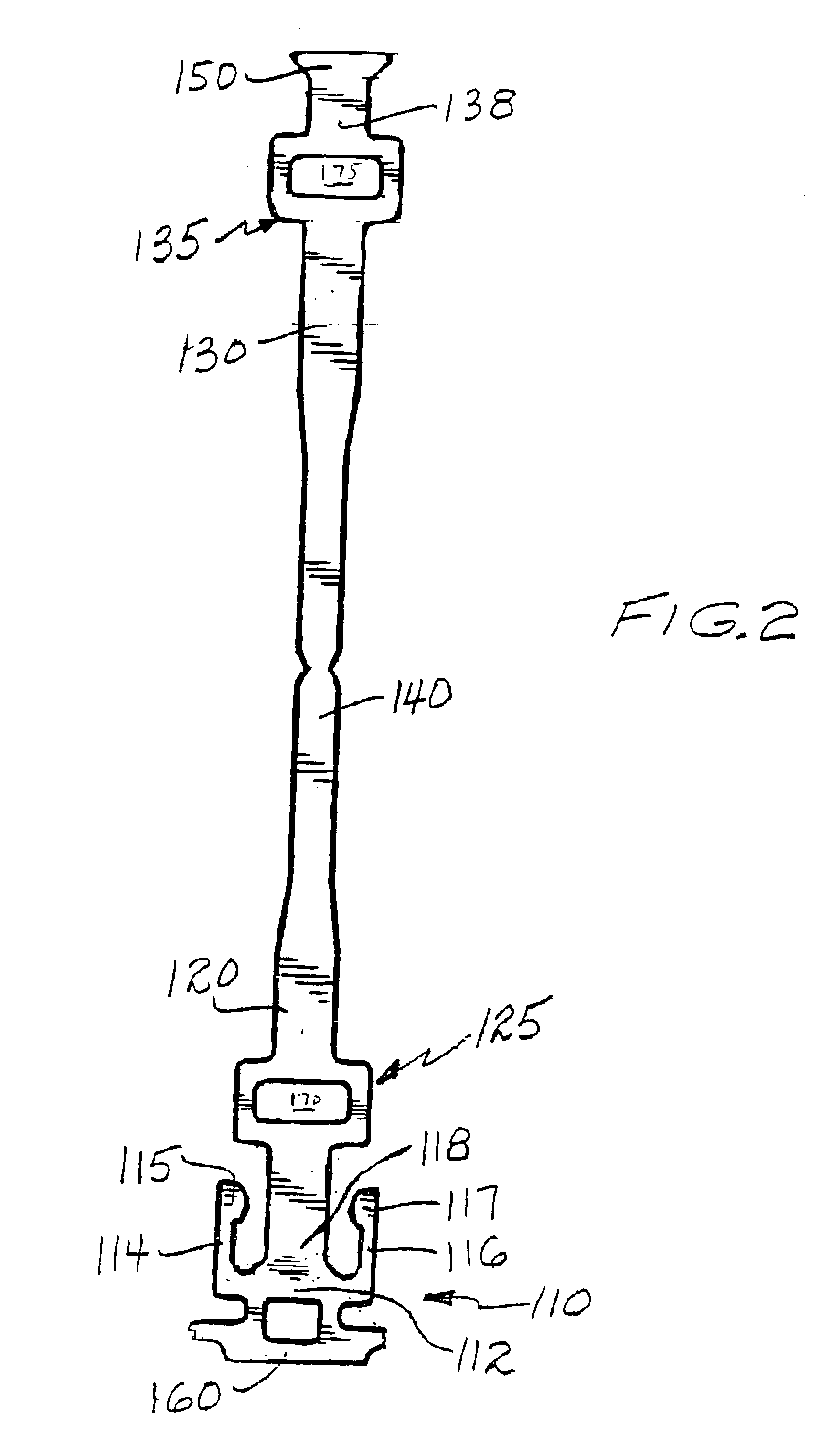
[0048]Referring again to FIGS. 1, 2, and 5, legs 120 and 130 are provided with openings 170 and 175, which are defined by deformable sections 125 and 135. These openings 170, 175 are adapted so as to break or stop capillary flow of solder within channel 180. The amount of solder that flows into channel 180 is primarily controlled by the placement of the lower of the two openings 170 and 175. More solder will flow into channel 180 when the lower opening is located farther away from base 110. Conversely, less solder will flow into channel 180 when the lower opening is located nearer to base 110. In the presently described first embodiment of electrical contact 100, opening 170 is the lower opening and may begin, for example, about 0.063 inch from base 110. Thus, solder will flow about 0.063 inch into channel 180 before being stopped by opening 170.

[0049]By controlling the amount of solder that flows into channel 180, the advantages of the capillary flow can be achieved without risking...


PUM


Abstract

There is provided electrical contact for circuit boards. Each leg of the pin section has a deformable segment that can expand or contract along the direction of the leg to alleviate stress created by relative movement of printed circuit boards and / or off-board components interconnected thereby. The deformable segments have members that project in opposing directions relative to the direction of the leg, so that the segments are symmetrical. In one embodiment, each leg has a deformable segment having a outwardly curved shape. In another embodiment, each leg has a deformable segment in the shape of a rectangular frame. The deformable segments define at least one opening where the two legs of the pin section are not overlapping, which breaks the capillary flow of solder between the legs. The amount of solder that flows into the electrical contact is selectively controlled by the selected placement of the deformable segments.

Description

BACKGROUND OF THE INVENTION[0001]1. Field of the Invention[0002]This invention pertains to electrical contacts. In particular, this invention pertains to electrical contacts between and for interconnecting spaced printed circuit boards (PCBs) and / or off-board components. The electrical contact includes a deformable segment adapted to alleviate stress on the connections with slight changes in the spacing between the PCBs.[0003]2. Description of the Related Art[0004]Numerous electrical contact designs have been developed for connecting a printed circuit board (hereinafter “PCB”) with off-board component and / or other PCBs. Representative contact designs include pins, posts, lugs, and tabs.[0005]Surface mounting technology (“SMT”) is a widely used method of securing electrical contacts to PCBs. This method includes providing an electrical contact to a “pick-and-place” machine, which picks up the electrical contact and places it at a predetermined position on a conductive pad or land on ...

Claims


Application Information

Patent Timeline
Patent Type & Authority Patents(United States)
IPC IPC(8): H01R13/64
CPCH01R12/57H01R13/6315H01R12/718H01R12/52H01R43/0256
Inventor LEGRADY, JANOSWOODS, WILLIAM L.LINDSEY, CLIFTON L.TRUONG, THANG D.MARTIN, JON P.LYTLE, RICHARD D.
Owner ZIERICK MFG
Why Eureka
Try Eureka