Lateral low-side and high-side high-voltage devices

a high-voltage device and low-side technology, applied in the direction of semiconductor devices, electrical equipment, transistors, etc., can solve the problems of high cost of hvics or pics, large area of high-voltage devices made by bcd technologies, and incompatible technologies employed. , to achieve the effect of small specific resistan

Active Publication Date: 2006-02-14
UNIV OF ELECTRONICS SCI & TECH OF CHINA
View PDF3 Cites 32 Cited by
  • Summary
  • Abstract
  • Description
  • Claims
  • Application Information

AI Technical Summary

Benefits of technology

[0018]The majority lateral devices using this invention has a advantage that the carriers used in the on-state are the electrons in the n-layer and / or the holes in the p-layer above the bottom p-layer. The bottom p-layer serves for sustaining the voltage to the substrate, whereas the layers above the bottom p-layer serves for the drifting of the carriers, due to that they are neutral in the conduction-state. Therefore, it provides a much smaller specific on-resistance.

Problems solved by technology

Therefore, the technologies employed are normally incompatible with conventional CMOS and BiCMOS technologies.
Furthermore, the areas of the high-voltage devices made by BCD technologies are normally large.
As a result, the costs of such HVICs or PICs are high.
However, the lateral power MOSTs, especially the lateral high-side power MOST made by such techniques has a large specific on-resistance.

Method used


Image

  • Lateral low-side and high-side high-voltage devices
  • Lateral low-side and high-side high-voltage devices
  • Lateral low-side and high-side high-voltage devices

Examples


Embodiment Construction

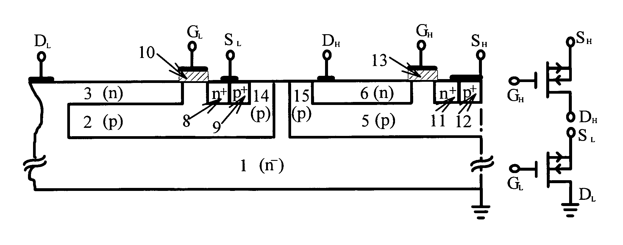
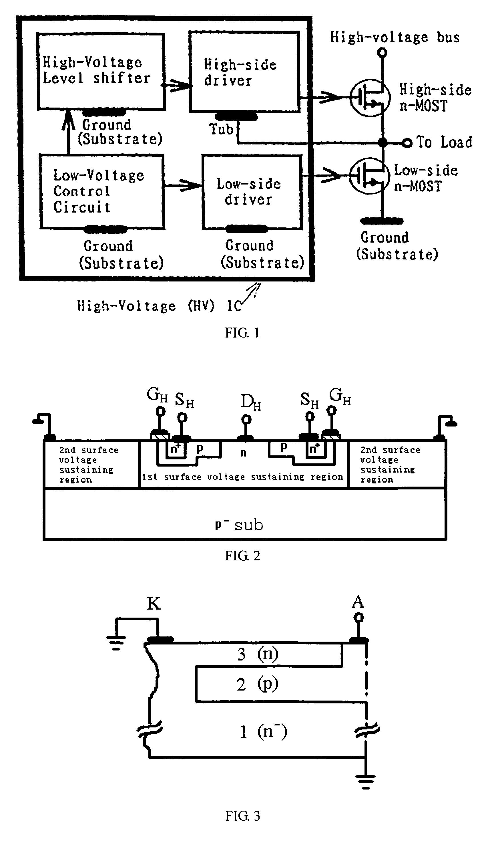
[0054]A reverse-biased p-n junction (diode) is the basis of most semiconductor devices, such as BJT, JFET and MOSFET. Therefore, the description of this invention is introduced by an explanation of the surface voltage-sustaining structures of the diode shown in FIG. 3 and FIG. 4.

[0055]Under a reverse biased condition, the diode shown in FIG. 3 sustains the voltage by a depletion region in the n-type substrate 1. The p-type layer 2 has a corresponding depletion region with opposite charges. The depletion region has a maximum width in the middle, i.e., on the dotted-dash line under the anode A, and a very small width under the cathode K. According to Ref. [4] and [5], the largest breakdown voltage can be achieved is 95% of that of a parallel plane abrupt junction by making the depleted acceptor density of p-layer 2 subtracted by the depleted donor density of n-layer 3 being a proper function of the distance from A (towards K).

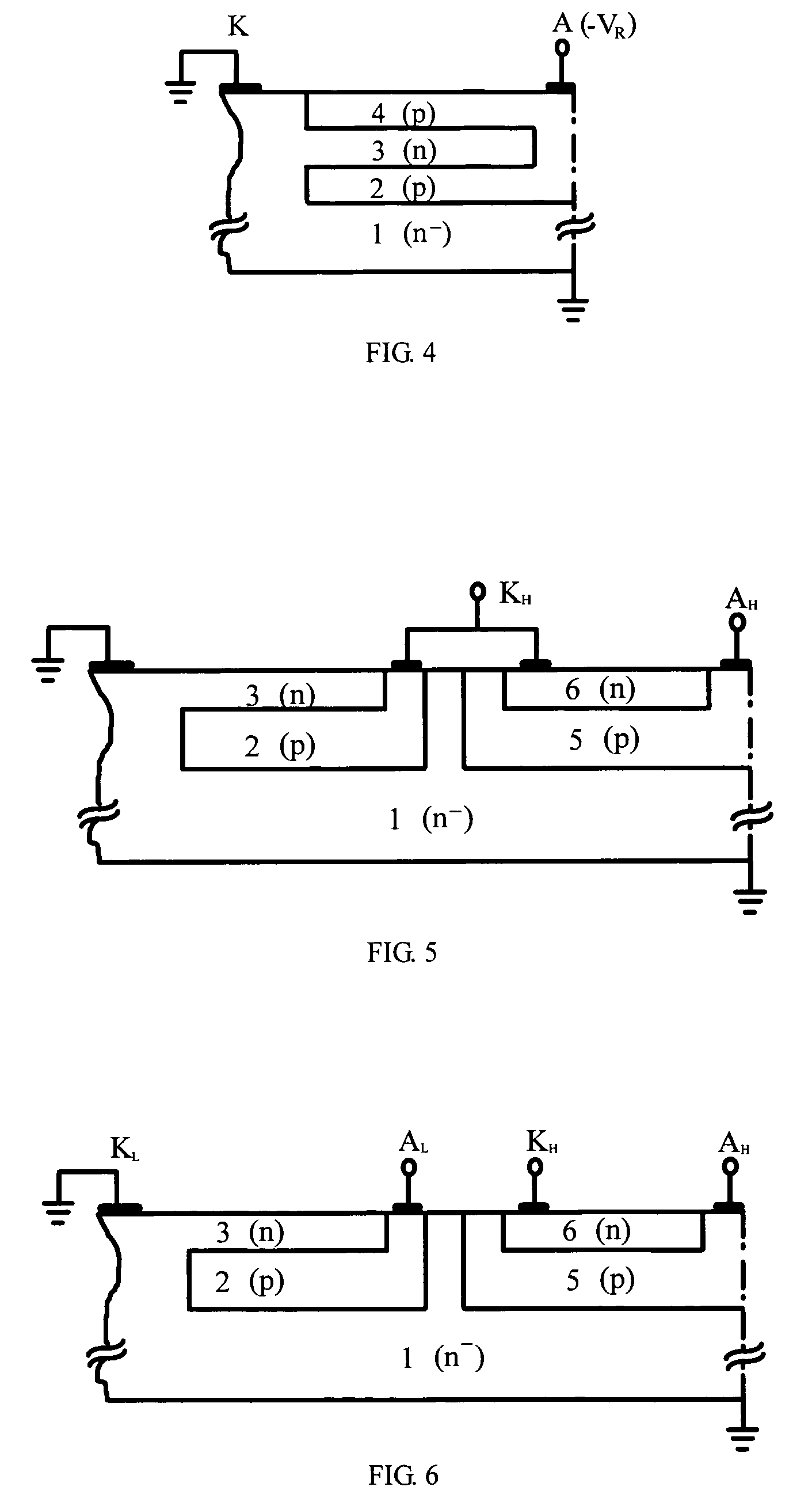
[0056]The same argument can be applied to FIG. 4. The diffe...


PUM


Abstract

Lateral high-side and low-side high-voltage devices with low specific on-resistances are made in a first and in a second surface voltage-sustaining region, respectively. In the on-state of high-side MOST (the right portion of the figure), the voltage across its source and its drain is very low and only layer 5 (p-type) is depleted to a large extent, layer 6 and layer 7 remain neutral and can serve as drift region(s) of electrons and / or holes. The drift region can be used for a single n-MOST or p-MOST, or even a parallel connection of n-MOST and p-MOST as shown in the figure. In the off-state of the high-side MOST, the voltage across its source and its drain is very large, but the voltage across its drain and the substrate 1 can be very low, and all of the layers in the first surface voltage-sustaining region are depleted, the depleted layer 5 produces an optimum variation lateral density of charge.The low-side MOST (the left portion of the figure) is similar to the high-side MOST.

Description

TECHNICAL FIELD[0001]The present invention relates to semiconductor high-voltage devices and high-power devices, more particularly to surface voltage-sustaining structure for lateral high-side and low-side high-voltage and high-power devices in High-Voltage Integrated Circuits (HVICs) and Power Integrated Circuits (PICs).BACKGROUND OF THE INVENTION[0002]As shown in FIG. 1, a conventional HVIC includes four portions: a low-voltage control circuit, a low-side driver connected to ground, a high-voltage level shifter and a high-side driver. The voltage of the tub shown in this figure can be varied from the voltage of the ground up to the voltage of the bus, which has a high-voltage related to the ground.[0003]In Ref. [1], the BCD techniques are presented for implementing the four circuits shown in the block of FIG. 1. However, DI and JI techniques must be used in BCD techniques. Therefore, the technologies employed are normally incompatible with conventional CMOS and BiCMOS technologies...

Claims


Application Information

Patent Timeline
Patent Type & Authority Patents(United States)
IPC IPC(8): H01L29/94H01L27/088H01L27/092H01L29/06H01L29/739H01L29/78
CPCH01L27/088H01L27/0928H01L29/7835H01L29/7393H01L29/7801H01L29/0634H01L29/7816
Inventor CHEN, XINGBI
Owner UNIV OF ELECTRONICS SCI & TECH OF CHINA
Why Eureka
Try Eureka