Semiconductor device having electrically erasable programmable read-only memory (EEPROM) and mask-ROM and method of fabricating the same

a technology of eeprom and maskrom, which is applied in the direction of semiconductor devices, transistors, electrical devices, etc., can solve the problems of increased harmful side effects of misalignment, and achieve the effect of reducing or preventing the misalignment of the tunnel oxide layer

Inactive Publication Date: 2006-03-07
SAMSUNG ELECTRONICS CO LTD
View PDF4 Cites 12 Cited by
  • Summary
  • Abstract
  • Description
  • Claims
  • Application Information

AI Technical Summary

Problems solved by technology

Where the EEPROM cell transistors have a plane-symmetrical structure, as may be the case in FIG. 4, for example, harmful side effects resulting from the misalignment may increase.

Method used


Image

  • Semiconductor device having electrically erasable programmable read-only memory (EEPROM) and mask-ROM and method of fabricating the same
  • Semiconductor device having electrically erasable programmable read-only memory (EEPROM) and mask-ROM and method of fabricating the same
  • Semiconductor device having electrically erasable programmable read-only memory (EEPROM) and mask-ROM and method of fabricating the same

Examples


Embodiment Construction

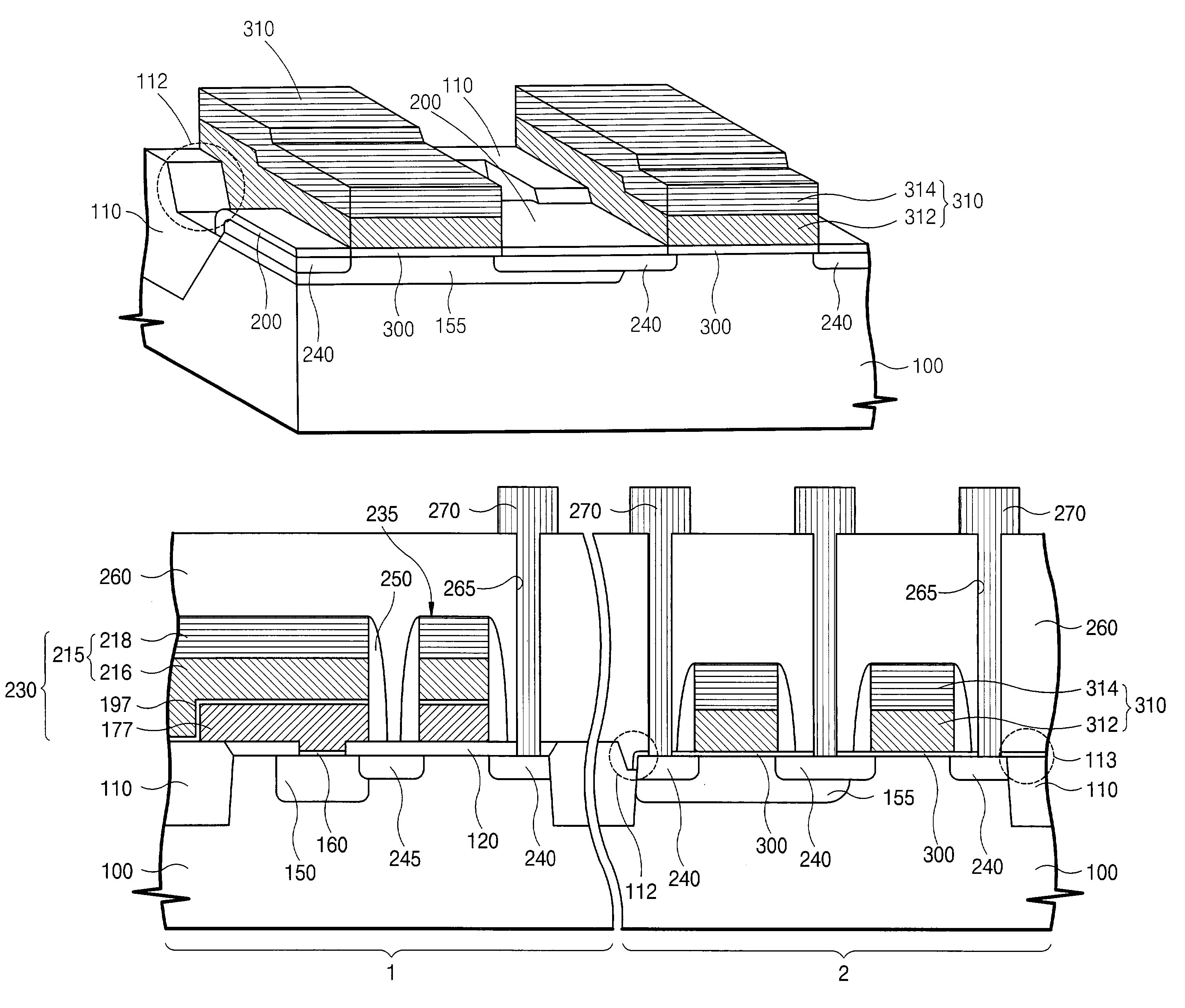
[0030]The present invention will now be described more fully hereinafter with reference to the accompanying drawings, in which exemplary embodiments of the invention are illustrated. The exemplary embodiments of the invention may, however, be embodied in different forms and should not be construed as limited to the exemplary embodiments set forth herein. Rather, these exemplary embodiments are provided so that this disclosure will be thorough and complete, and will fully convey the scope of the invention to those skilled in the art. In the drawings, the thickness of layers and regions are exaggerated for clarity. It should be understood that when a layer is referred to as being “on” another layer or substrate, it can be adjacent, directly on and / or directly adjacent to the other layer or substrate, interposed between layers, or intervening layers may also be present between the layers and the other layer or substrate. Like numbers refer to like elements throughout.

[0031]FIGS. 5 and ...


PUM


Abstract

A semiconductor device including an EEPROM and a Mask-ROM transistor, and methods of fabricating and forming the same, where a device isolation layer may be formed at given regions of a semiconductor substrate to define a cell active region, and a Mask-ROM active region including a channel doped region therein. A channel doped region may be formed within the Mask-ROM active region, and a plurality of Mask-ROM gates may be formed that cross the channel doped region. A Mask-ROM gate insulating layer may be interposed between a Mask-ROM gate and the Mask-ROM active region, and the device isolation layer may have a surface adjacent to the channel doped region that is lower as compared to a surface of the device isolation layer that is not directly adjacent to the channel doped region.

Description

CROSS-REFERENCE TO RELATED CASES[0001]This U.S. nonprovisional patent application claims priority under 35 U.S.C. § 119 of Korean Patent Application 2002-48044 filed on Aug. 14, 2002, the entire contents of which are hereby incorporated by reference.BACKGROUND OF THE INVENTION[0002]1. Field of the Invention[0003]The present invention relates to a semiconductor device having an EEPROM transistor and a Mask-ROM transistor, and methods of fabricating and forming the same.[0004]2. Description of the Related Art[0005]A smart card may be used as an identification card, as a credit card and as electronic cash. These uses are continuously increasing. The smart card embeds user information and transaction information and simultaneously embeds a program suitable for its purpose. Accordingly, the smart card embeds nonvolatile memory transistors for writing and storing the user information and transaction information, and includes Mask-ROM transistors for coding the program. The nonvolatile mem...

Claims


Application Information

Patent Timeline
Patent Type & Authority Patents(United States)
IPC IPC(8): H01L21/336H01L27/088H01L21/8234H01L21/8246H01L21/8247H01L27/10H01L27/105H01L27/112H01L27/115H01L29/788H01L29/792
CPCH01L27/105H01L27/112H01L27/11246H01L27/1126H01L27/11526H01L27/115H01L27/11521H01L27/11524H01L27/11293H10B20/367H10B20/383H10B20/65H10B20/00H10B41/40H10B69/00H10B41/30H10B41/35
Inventor PARK, WEON-HO
Owner SAMSUNG ELECTRONICS CO LTD
Why Eureka
Try Eureka