Semiconductor memory device including a flash memory cell array and a mask read-only memory cell array

a memory cell array and memory chip technology, applied in semiconductor devices, digital storage, instruments, etc., can solve the problems of leaking program information, affecting the degree of integration of semiconductor memory devices, and requiring a lot of time to confirm, so as to improve the integration degree of system-on-chip or microcomputer chips, the effect of reducing the time required

Inactive Publication Date: 2007-06-12
SAMSUNG ELECTRONICS CO LTD
View PDF9 Cites 10 Cited by
  • Summary
  • Abstract
  • Description
  • Claims
  • Application Information

AI Technical Summary

Benefits of technology

[0014]Embodiments of the present invention relate to a semiconductor memory device or method of manufacturing a semiconductor device, which can improve the degree of integration of a system-on-chip (SOC) or a microcomputer chip. Embodiments efficiently prevent information on programs coded in a mask read-only memory (ROM) from being leaked and / or reduce the time required for processing ranging from design of the mask ROM to production of the finished product.

Problems solved by technology

Such structures may be obstacles to improvements in the degree of integration of semiconductor memory devices.
When the mask ROM block and the EEPROM block are formed separately, there is the possibility of leaking information of the programs.
As a result, the repeated testing requires a lot of time to confirm if the mask ROM is correctly executing, to ensure reliability.

Method used


Image

  • Semiconductor memory device including a flash memory cell array and a mask read-only memory cell array
  • Semiconductor memory device including a flash memory cell array and a mask read-only memory cell array
  • Semiconductor memory device including a flash memory cell array and a mask read-only memory cell array

Examples


Embodiment Construction

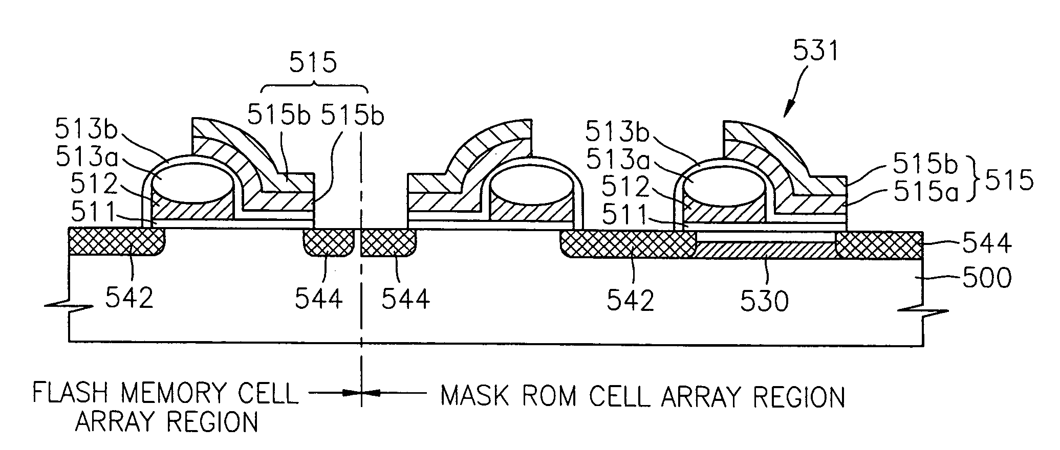
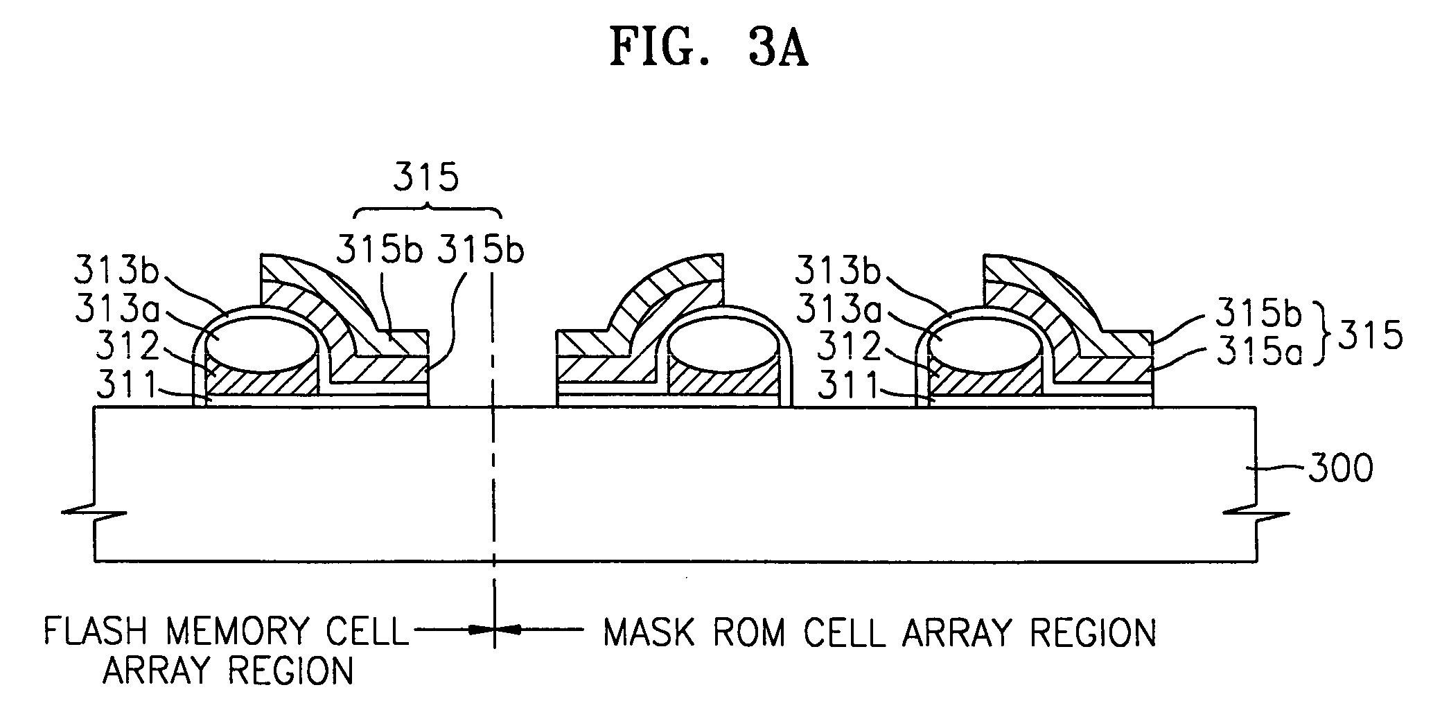
[0028]FIGS. 3A through 3D are example schematic cross-sections of a semiconductor memory device according to embodiments of the present invention and a method of manufacturing the semiconductor memory device.

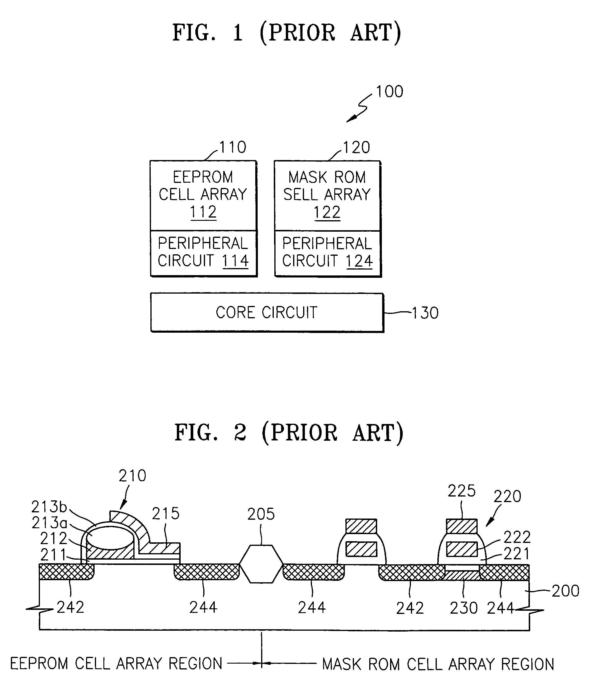
[0029]Referring to FIG. 3A, a plurality of gate structures are formed on the semiconductor substrate 300 on which a flash memory region and a mask read-only memory (ROM) region are defined. The flash memory region is a region on which a flash memory unit and its peripheral circuit are formed. The mask ROM region is a region on which a mask ROM unit and its peripheral circuit are formed. In embodiments, each of the gate structures of the flash memory region and the mask ROM region are split gate structures.

[0030]The split gate structure may be formed by the following steps. A first oxide layer is formed on the entire surface of the semiconductor substrate 300 to form a gate oxide layer. For example, the first oxide layer may be formed by thermally oxidizing the semiconductor subs...


PUM


Abstract

A semiconductor memory device included in a system-on-chip (SOC) or a microcomputer chip. The semiconductor memory device may include a flash memory cell array unit and a mask read-only memory (ROM) cell array unit which are formed in a single memory block without an isolation layer for separating the two units. Transistors included in the flash memory unit and the mask ROM unit are the same type and may have two threshold voltages. The transistor in each memory cell unit may be a split gate transistor, a metal-oxide-nitride-oxide-silicon, or silicon-oxide-nitride-oxide-silicon transistor. Further, the transistor included in the mask ROM unit in the semiconductor memory device may include enhancement transistors or depletion transistors in which a dopant ion-implanted region is formed at channel portions.

Description

BACKGROUND OF THE INVENTION[0001]1. Field of the Invention[0002]Embodiments of the present invention relate to a semiconductor memory device including a flash memory cell array and a mask read-only memory (ROM) cell array and a method of manufacturing the semiconductor memory device.[0003]This application claims the priority of Korean Patent Application No. 2003-44544, filed on Jul. 2, 2003, in the Korean Intellectual Property Office, the disclosure of which is incorporated herein in its entirety by reference.[0004]2. Description of the Related Art[0005]System-on-chips (SOCs) integrate essential system functions onto one chip. Since both hardware and software are merged and both analog and digital are integrated in the SOCs, a single semiconductor chip can operate as a system. In other words, SOCs can contain all functions in a single semiconductor chip, such as memory, non-memory (large scale integrated circuit (LSI)), analog components, digital components, hardware, and software. ...

Claims


Application Information

Patent Timeline
Patent Type & Authority Patents(United States)
IPC IPC(8): H01L29/76H01L27/112H01L21/336H01L21/8234H01L21/8246H01L21/8247H01L27/105
CPCH01L27/105H01L27/112H01L27/1126H01L27/11293H01L27/11521H01L27/11526H10B20/383H10B20/65H10B20/00H10B41/40H10B41/30
Inventor MIN, HONG-KOOKKIM, YONG-TAE
Owner SAMSUNG ELECTRONICS CO LTD
Why Eureka
Try Eureka