Process for manufacturing integrated circuit on a substrate

A manufacturing method, integrated circuit technology, applied in the direction of circuit, semiconductor/solid-state device manufacturing, electrical components, etc., can solve the problem that the transistor channel cannot be effectively shortened

Inactive Publication Date: 2004-08-18
MACRONIX INT CO LTD
View PDF0 Cites 10 Cited by
  • Summary
  • Abstract
  • Description
  • Claims
  • Application Information

AI Technical Summary

Problems solved by technology

However, today's oxidation and high-temperature heat flow method implants dopants, and the diffusion caused by them cannot effectively shorten the channel of the transistor.

Method used


Image

  • Process for manufacturing integrated circuit on a substrate
  • Process for manufacturing integrated circuit on a substrate
  • Process for manufacturing integrated circuit on a substrate

Examples


Embodiment Construction

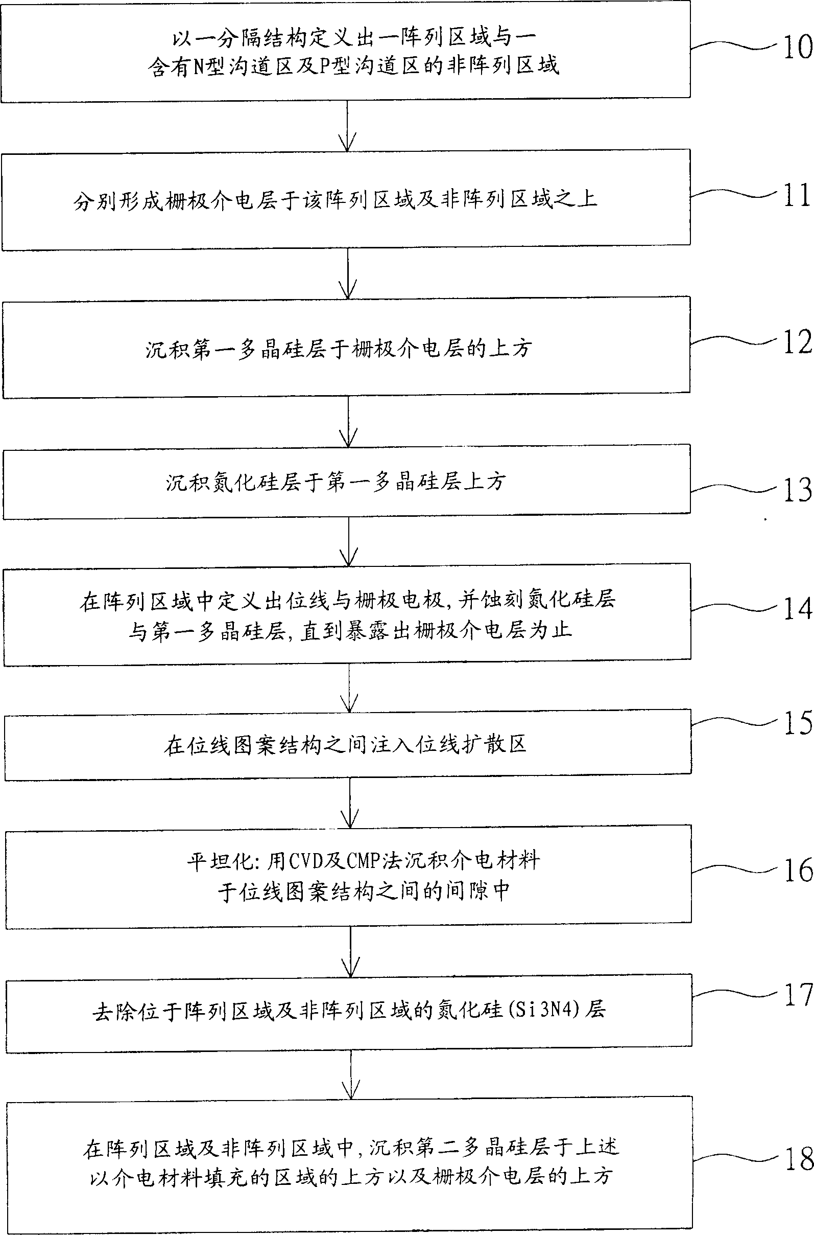
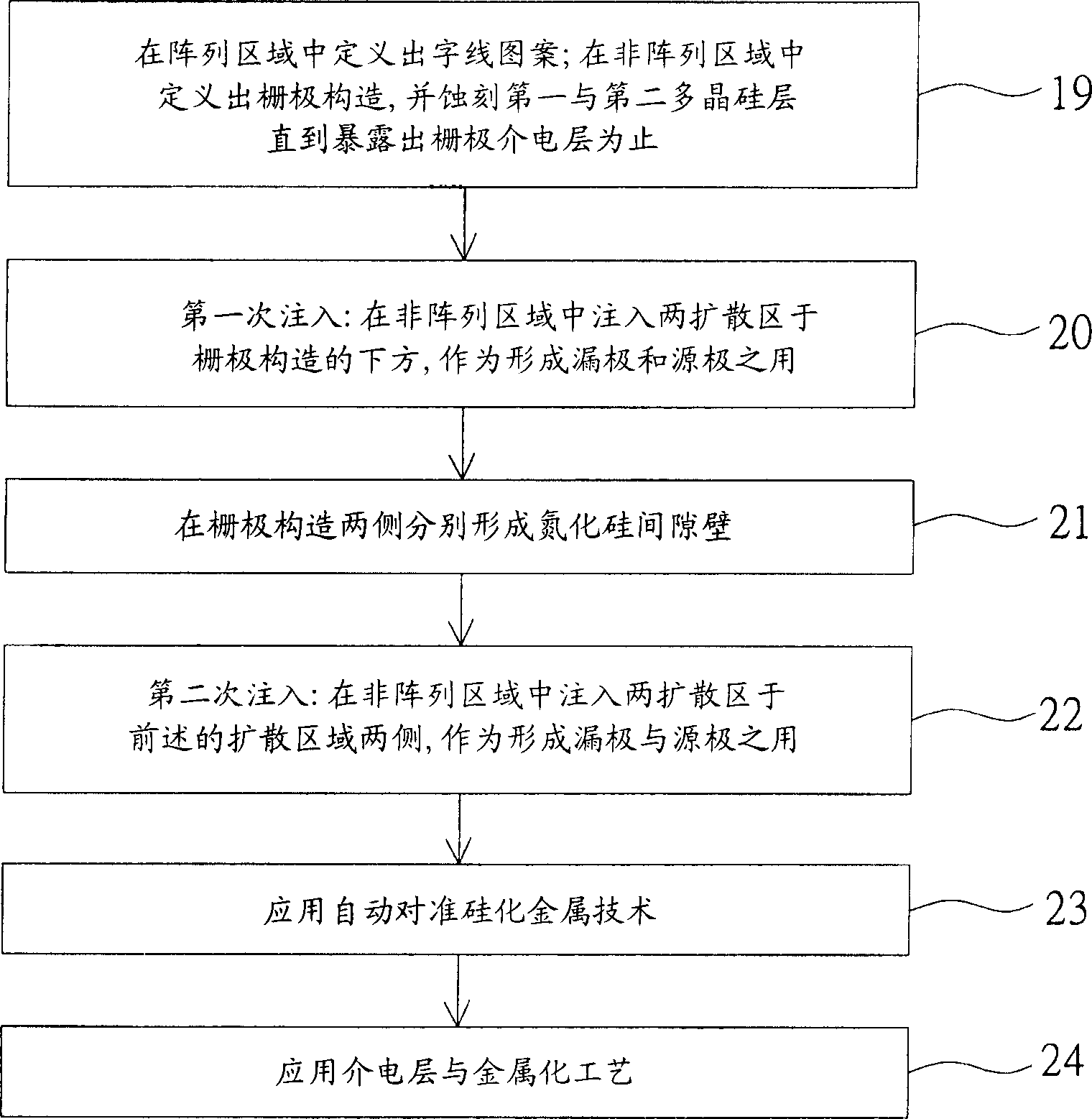
[0040] The manufacturing method disclosed in the present invention will be described in detail as follows with examples and accompanying drawings. Figure 1A-1B is a flowchart of a manufacturing method according to an embodiment of the present invention. Figure 2-10 is according to Figure 1A-1B The block diagram of the hybrid integrated circuit with embedded mask memory shown in the steps. and Figure 11 is the application Figure 2-10 Block diagram of embedded non-volatile memory with SONOS memory for process technology.

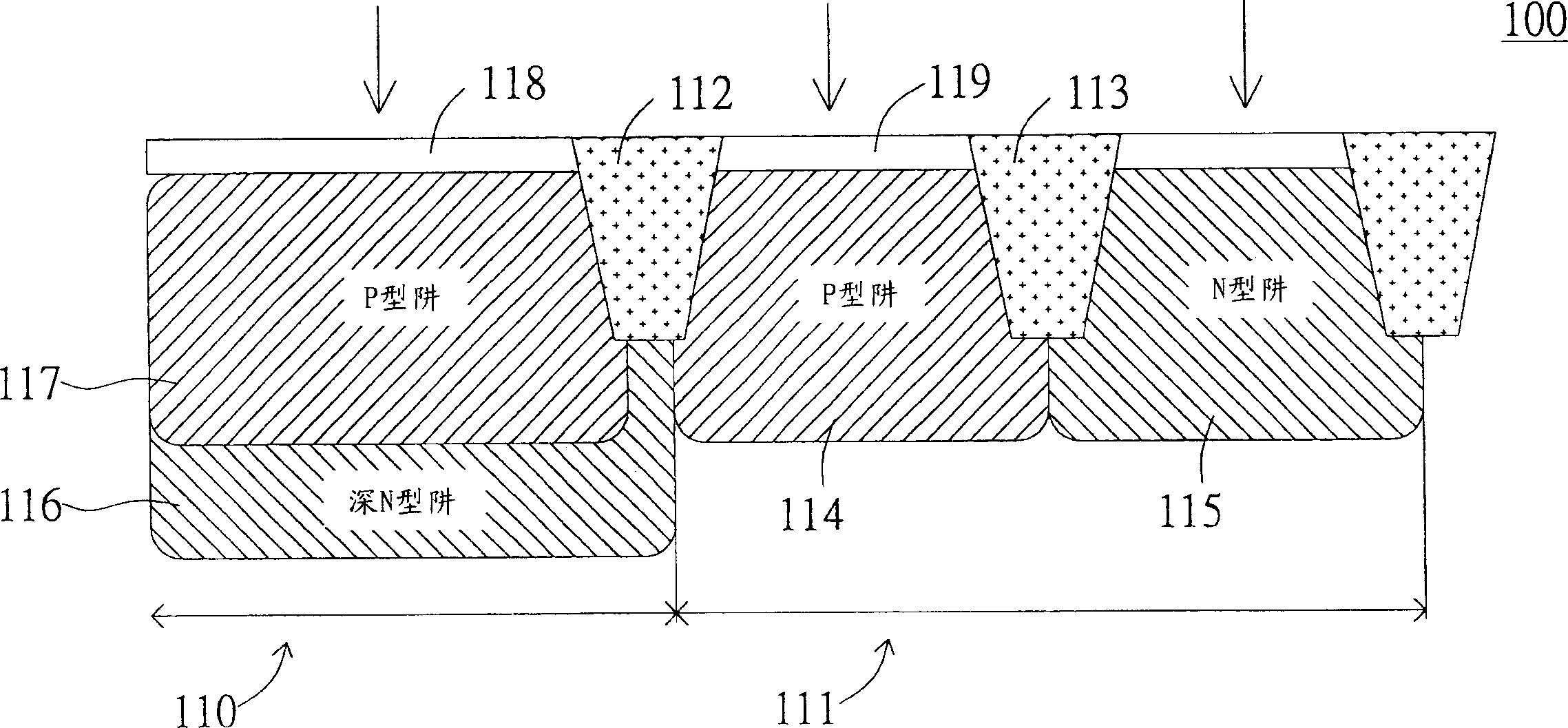
[0041] Please refer to Figure 1A-1B , each step is arranged in numerical order from step block 10 to step block 24 to illustrate the manufacturing method of the present invention. First, as described in step block 10 , the substrate is separated by a dielectric region 112 to define an array region 110 and a non-array region 111 . like figure 2 As shown, the dielectric region 112 is formed on the substrate by filling a trench with oxide or other diel...


PUM


Abstract

A process uses two layers of polysilicon for fabricating high-density nonvolatile memory, such as mask ROM or SONOS memory, integrated with advanced peripheral logic on a single chip. The method includes covering a gate dielectric layer with a first layer of polysilicon in the array portion and in the non-array portion; covering the first layer of polysilicon with a layer of silicon nitride; using two masks for gate electrode formation in a first layer of polysilicon and bit line implant processes; depositing a dielectric material among the gate electrode structures to fill gaps among the gate structures; planarizing the deposited oxide; removing said layer of silicon nitride and applying a second layer of polysilicon material; patterning wordlines in the array portion over said gate electrode structures, and transistor gate structures in said non-array portion, and applying LDD, silicide and other logic circuit processes.

Description

technical field [0001] The invention relates to a method for manufacturing integrated circuits on a substrate, in particular to a method for manufacturing nonvolatile memories with tiny critical dimensions, and in particular to an embedded nonvolatile memory suitable for composite integrated circuits Method for manufacturing sexual memory. Background technique [0002] With the advancement of the manufacturing technology of integrated circuits, the size of components on the integrated circuit is gradually reduced, and the degree of integration of functions on a single chip is also gradually increased. Therefore, there are many embedded non-volatile memory chips containing logic functional elements, such as memory controllers, general-purpose processors, input / output interface logic ), dedicated logic, digital signal processors, and various chips with other functions. [0003] At present, there are still some problems to be solved in the design and process of the composite ...

Claims


Application Information

Patent Timeline
Patent Type & Authority Applications(China)
IPC IPC(8): H01L21/8246H01L27/112H01L27/115
CPCH01L27/11253H01L27/112H01L27/115H01L27/11568H10B20/38H10B20/00H10B43/30H10B69/00
Inventor 黄仲仁
Owner MACRONIX INT CO LTD
Why Eureka
Try Eureka