

Method for manufacturing imbedded non-volatile memory with sacrificed layer
A manufacturing method, polysilicon layer technology, applied in semiconductor/solid-state device manufacturing, electrical components, circuits, etc., can solve problems such as inability to effectively shorten transistor channels
- Summary
- Abstract
- Description
- Claims
- Application Information
AI Technical Summary
Problems solved by technology
Method used
Image

Examples
Embodiment Construction
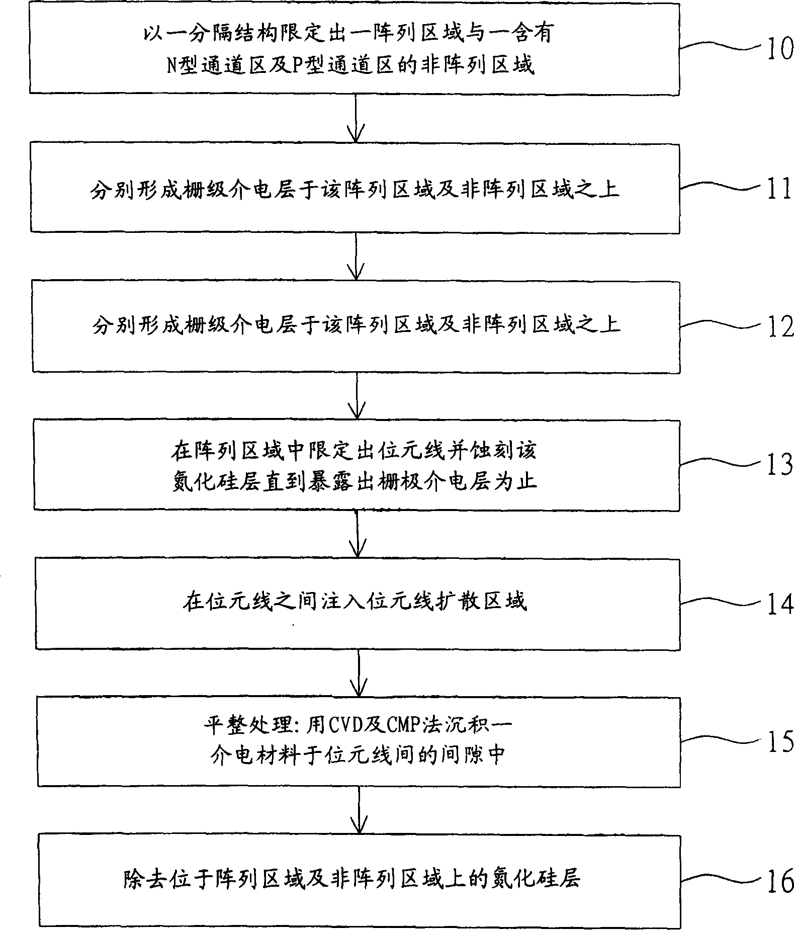
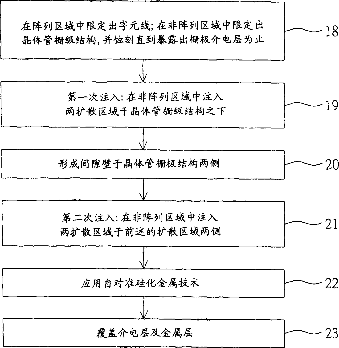
[0057] The detailed manufacturing method and practical application disclosed in the present invention will be described as follows with reference to the accompanying drawings. Figure 1A ~ Figure 1B It is a flowchart of a manufacturing method drawn according to an embodiment of the present invention. Figure 2 to Figure 10 Illustrated structure diagram of Figure 1A ~ Figure 1B related steps. and Figure 11 It is a sectional view of an embedded non-volatile memory structure with a SONOS memory unit drawn by applying the present invention.
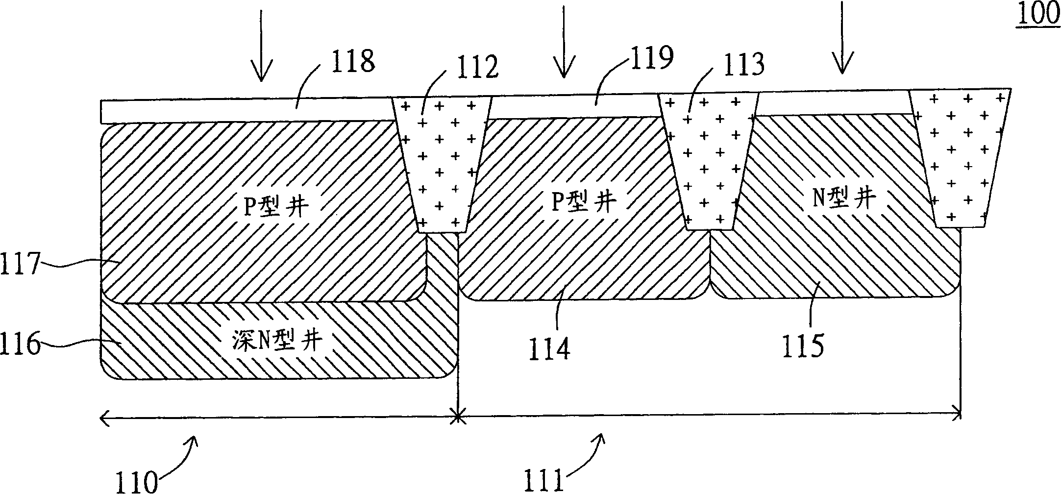
[0058] Please refer to Figure 1A ~ Figure 1B , each step will be described in numerical order from step block 10 to step block 23 to illustrate the manufacturing method of the present invention. First, as described in step block 10 , a dielectric region 112 is used on the substrate 100 to separate the substrate 100 to define an array area 110 and a non-array area 111 . As shown in FIG. 2, the dielectric region 112 is formed on the substr...
PUM
| Property | Measurement | Unit |
|---|---|---|
| Thickness | aaaaa | aaaaa |
| Thickness | aaaaa | aaaaa |
| Thickness | aaaaa | aaaaa |
Abstract
Description
Claims
Application Information