Semiconductor device with mask read-only memory and method of fabricating the same

a read-only memory and semiconductor technology, applied in the direction of instruments, transistors, alphabetical characters entering, etc., can solve the problems of high manufacturing cost, inconvenient use of high-energy ion implantation process, and abnormal operation of the device, so as to reduce the change of threshold voltage and low cost

Inactive Publication Date: 2007-07-12
SAMSUNG ELECTRONICS CO LTD
View PDF5 Cites 10 Cited by
  • Summary
  • Abstract
  • Description
  • Claims
  • Application Information

AI Technical Summary

Benefits of technology

[0012]Embodiments of the present invention are also directed to a method of fabricating an EML semiconductor device with a mask ROM in low cost.
[0013]Embodiments of the present invention are further directed to a mask ROM device capable of reducing a change of threshold

Problems solved by technology

However, as the high implantation energy may result in an increased diffusion length of the impurities, the ionic impurities injected with high energy may thus be diffused to an adjacent transistor during the subsequent processing step.
Consequently, the above-mentioned inadvertent diffusion of impurities may result in a threshold voltage change for the adjacent transistor, which in turn may cause an abnormal operation for the device.
Furthermore, as the impurit

Method used


Image

  • Semiconductor device with mask read-only memory and method of fabricating the same
  • Semiconductor device with mask read-only memory and method of fabricating the same
  • Semiconductor device with mask read-only memory and method of fabricating the same

Examples


Embodiment Construction

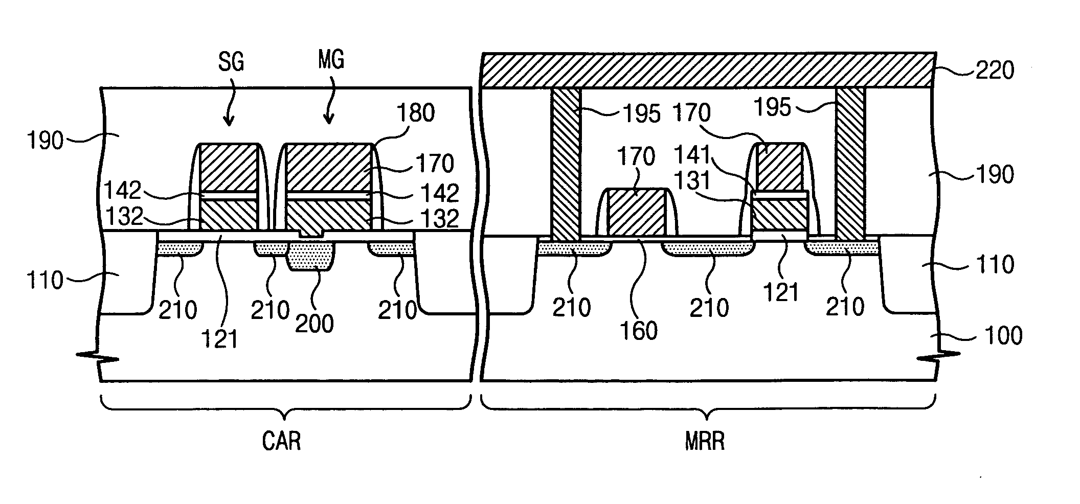
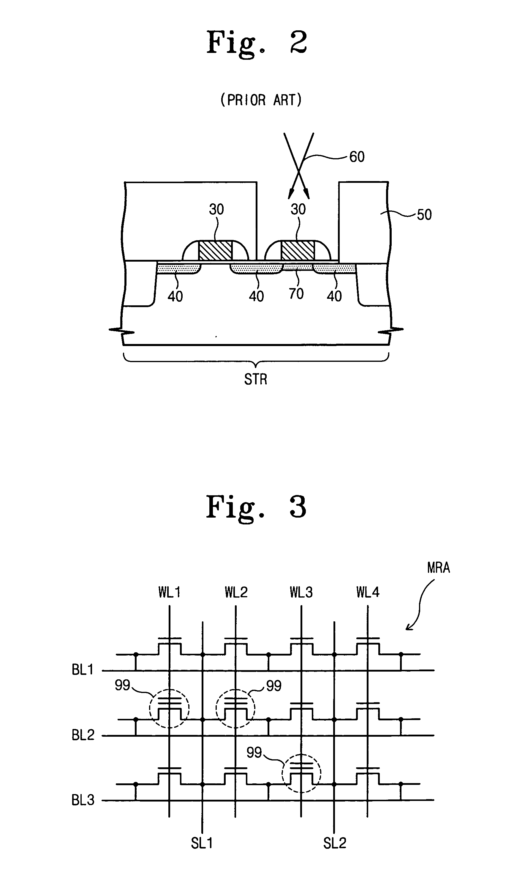
[0044]Preferred embodiments of the present invention will be described below in more detail with reference to the accompanying drawings. The present invention may, however, be embodied in different forms and should not be constructed as limited to the preferred embodiments set forth herein.

[0045]In the figures, the dimensions of layers and regions are exaggerated for clarity of illustration. It will also be understood that when a layer (or layer) is referred to as being ‘on’ another layer or substrate, it can be directly on the other layer or substrate, or intervening layers may also be present. Further, it will be understood that when a layer is referred to as being ‘under’ another layer, it can be directly under, and one or more intervening layers may also be present. In addition, it will also be understood that when a layer is referred to as being ‘between’ two layers, it can be the only layer between the two layers, or one or more intervening layers may also be present. Like ref...


PUM


Abstract

A mask read only memory (ROM) device includes a plurality of isolation patterns disposed at predetermined regions of a semiconductor substrate to define a plurality of active regions. The semiconductor substrate includes a mask ROM region where a plurality of on cells and a plurality of off-cells are disposed. The mask ROM further includes a plurality of gate lines disposed over the active regions, and which cross over the isolation patterns, a plurality of gate insulating layers interposed between the gate lines and the active regions and a floating conductive pattern and a inter-gate dielectric pattern located between the gate line and the gate insulating layer of the off-cell.

Description

CROSS-REFERENCE TO RELATED APPLICATIONS[0001]This U.S. non-provisional patent application claims priority under 35 U.S.C. § 119 of Korean Patent Application No. 2006-01891 filed on Jan. 6, 2006, the disclosure of which is hereby incorporated by reference herein in its entirety.BACKGROUND[0002]1. Technical Field[0003]The present disclosure relates to semiconductor devices and method of fabricating the same and in particular relates to a semiconductor device with a mask read-only memory (mask ROM) and to a method of fabricating the same.[0004]2. Discussion of the Related Art[0005]Due to the popularization of portable electronic apparatuses such as, for example, mobile phones, personal digital assistants (PDA), digital cameras, camcorders, gaming machines, there has been an increasing demand for embedded-memory-and-logic (EML) semiconductor device equipped with memories and logic circuits on a single chip.[0006]FIG. 1 shows a chip layout pattern of an EML semiconductor device as an exa...

Claims


Application Information

Patent Timeline
IPC IPC(8): H01L29/788H01L21/336
CPCG11C17/12H01L27/0207H01L27/105H01L27/11246H01L27/11253H01L27/11546H01L27/11286H01L27/11293H01L27/11519H01L27/11526H01L27/1126H10B20/367H10B20/38H10B20/383H10B20/60H10B20/65H10B41/10H10B41/40H10B41/49H04M1/23G06F3/0233H04M2250/70
Inventor YANG, SEUNG-JINHAN, JEONG-UK
Owner SAMSUNG ELECTRONICS CO LTD
Why Eureka
Try Eureka