

Semiconductor memory device
a memory device and semiconductor technology, applied in the field of semiconductor storage devices, can solve the problems of reducing the power consumption of devices, obstructing the enhancement of the throughput of data processors, and difficult to form a large capacity sram, and achieve the effect of secure capacitance and effective application
- Summary
- Abstract
- Description
- Claims
- Application Information
AI Technical Summary
Benefits of technology
Problems solved by technology
Method used
Image

Examples
first embodiment
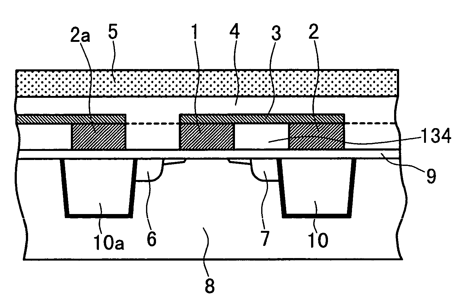
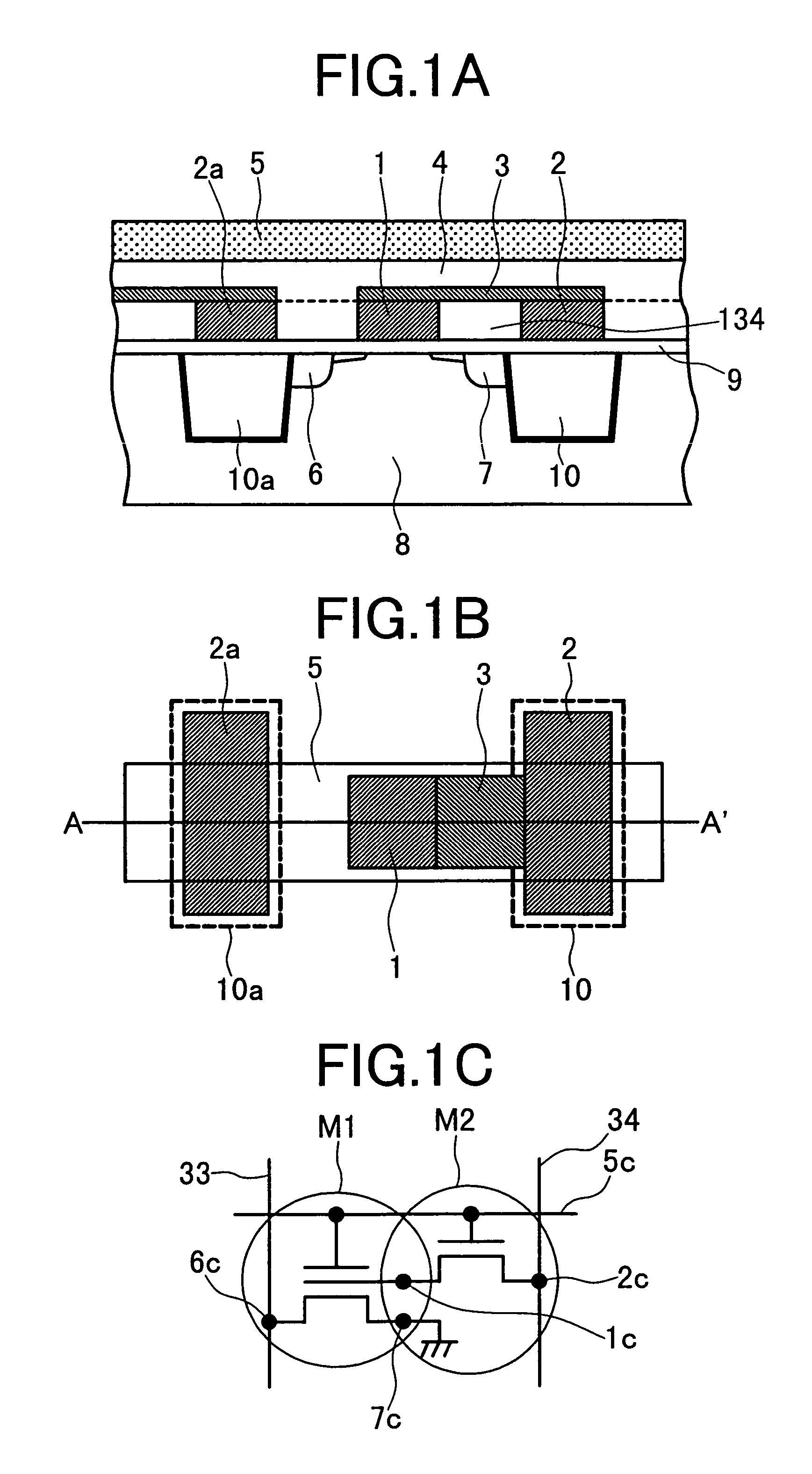
[0076]A semiconductor memory device in a first embodiment according to the present invention is formed on a semiconductor substrate. FIGS. 1(a), 1(b) and 1(c) are, respectively, a sectional view, a top view and a circuit diagram of an equivalent circuit of a memory cell included in the semiconductor memory device in the first embodiment. In FIG. 1(b), some parts of the overlapping outlines of regions are shifted relative to each other to facilitate understanding, and components shown in FIGS. 1(a) to 1(c) correspond with each other. FIG. 1(b) shows the positional relationship between the principal parts of the memory cell but does not accurately show layers.
[0077]Basically, the memory cell is integrally provided with a write transistor M2 for writing information and a read transistor M1 for reading stored information. The memory cell is the so-called gain cell structure including thin-film FETs (field effect transistors).
[0078]The write transistor M2 is a thin-film FET. The concentr...
second embodiment
[0108]FIG. 8(a) is a typical sectional view of a memory cell included in a semiconductor memory device in the second embodiment according to the present invention, and FIG. 8(b) is a top view of the memory cell shown in FIG. 8(a). The memory cell of the second embodiment is basically the same in configuration as the memory cell of the first embodiment, except that the memory cell of the second embodiment is formed on a SOI substrate (silicon-on-insulator substrate). Hence, the gate electrode of the read transistor of the memory cell of the second embodiment, the method of forming the gate electrode of the read transistor, and the thickness of a film forming the channel of the write transistor of the memory cell of the second embodiment are different from those of the memory cell of the first embodiment. Many processes for fabricating the logic circuit of the second embodiment can be used also for fabricating the memory cells of the second embodiment, and only a few additional proces...
third embodiment
[0129]In the first and second embodiments, the drain regions of the plurality of read transistors are connected by the diffused layer. In the third embodiment, memory cells are connected to contacts 113, respectively, and the contacts 113 are connected to a read data line 109, included in an upper wiring layer. The two memory cells share the one contact 113. Although the area of a region in which memory cells are arranged is small when a diffused layer is used, source lines 114 having a small parasitic resistance and permitting quick access are connected by a diffused layer and are extended parallel to word lines 106.
[0130]FIGS. 22 to 24 are views for explaining the third embodiment. FIGS. 22(a) and 22(b) are typical sectional views, FIG. 23 is a top view of the memory cell array of the third embodiment, and FIG. 24 is a circuit diagram of an equivalent circuit of the memory cell array of the third embodiment. FIG. 22(a) is a sectional view taken on line L–L′ in FIG. 23, and FIG. 22...
PUM
 Abstract
Description
Claims
Application Information