MRAM and data writing method therefor

a data writing and random access memory technology, applied in the field of magnetic random access memory and data writing method therefor, can solve the problems of increasing the delay in response when data is read out therefrom, and gradually increasing the importance of problems, and achieve the effect of a new array structur

Active Publication Date: 2006-03-07
RENESAS ELECTRONICS CORP
View PDF7 Cites 4 Cited by
  • Summary
  • Abstract
  • Description
  • Claims
  • Application Information

AI Technical Summary

Benefits of technology

[0021]In the light of the foregoing, it is, therefore, an object of the present invention to provide a magnetic memory (MRAM) having memory cells formed using tunnel magneto-resistance elements (TMR elements) which is capable of realizing a novel array structure, an operation thereof, and more miniature planar layout.

Problems solved by technology

As a result a value of a detected current caused to flow when data is read out from a memory cell becomes small or a delay in response when data is read out therefrom is increased.
Thus, this problem has gradually become important.
If a method of dividing a conventional memory cell array into blocks is introduced in order to avoid the above-mentioned problem, there may be encountered a problem as will be described below.

Method used


Image

  • MRAM and data writing method therefor
  • MRAM and data writing method therefor
  • MRAM and data writing method therefor

Examples


first embodiment

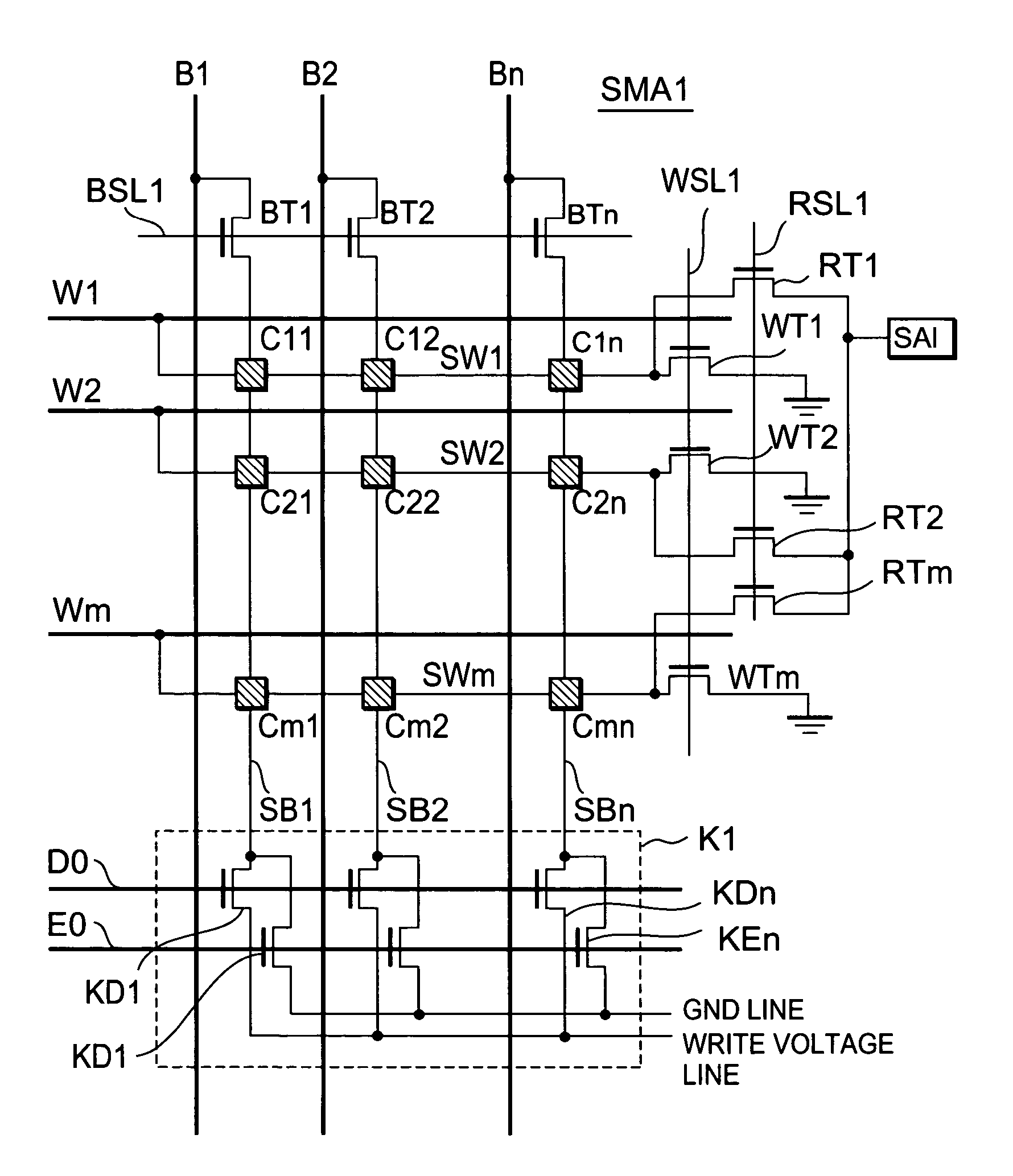
[0040]FIG. 1 is a circuit diagram showing a sub-memory cell array SMA1 of an MRAM according to the present invention.

[0041]The sub-memory cell array SMA1 includes a plurality of main word lines W1 to Wm (m: a natural number equal to or larger than 2), and a plurality of main bit lines B1 to Bn (n: a natural number equal to or larger than 2). The main word lines W1 to Wm are distributed so as to intersect the main bit lines B1 to Bn.

[0042]Sub-word lines SW1 to SWm are distributed in parallel with the main word lines W1 to WM, respectively. One ends of the sub-word lines SW1 to SWm are connected to the corresponding main word lines W1 to Wn, respectively, and the other ends thereof are connected to corresponding one ends (corresponding drain terminals) of word line selecting transistors WT1 to WTm for selecting one of word lines in sub-memory cell arrays, respectively. All gates of the word line selecting transistors WT1 to WTm are connected to a first word line selecting line WSL1. A...


PUM


Abstract

In an MRAM having main and sub-structures, selecting transistors are arranged so as to meet the arrangement order of main word lines, sub-word lines and the selecting transistors. The selecting transistor is driven to cause a snap back phenomenon to occur. As a result, data can be written to a memory cell using a substrate current, not a channel current. Moreover, a data may be written into a selected memory cell by discharge the charge which is charged in the main and sub word lines corresponding to the memory cell.

Description

BACKGROUND OF THE INVENTION[0001]1. Field of the Invention[0002]The present invention relates to a magnetic random access memory (MRAM) and a data writing method therefor.[0003]2. Related Background Art[0004]In recent years, an MRAM which has highly densely integrated magnetic substances on a substrate as memory cells, and which has nonvolatile characteristics, a high speed operation and repetition resistance of magnetic recording, has been expected as a next generation memory.[0005]FIGS. 7A and 7B are perspective views each useful in explaining a basic structure and an operation of a memory cell of an MRAM.[0006]As shown in FIG. 7A, an MRAM cell includes a pinned layer 12 made of a ferromagnetic film and having a fixed magnetization direction, an insulating film 13 and a data storage layer 14 made of a ferromagnetic film. The MRAM cell is provided between a lower wiring 11 and an upper wiring 15.[0007]FIG. 7B is a perspective view useful in explaining the operation for writing and ...

Claims


Application Information

Patent Timeline
Patent Type & Authority Patents(United States)
IPC IPC(8): G11C11/14G11C11/15G11C11/16H01L21/8246H01L27/105H01L43/08
CPCG11C11/16G11C5/025G11C7/18G11C8/14G11C11/1675
Inventor OKAZAWA, TAKESHI
Owner RENESAS ELECTRONICS CORP
Why Eureka
Try Eureka