Check patentability & draft patents in minutes with Patsnap Eureka AI!

Built-in test support for an integrated circuit

a technology of integrated circuits and integrated circuits, applied in the direction of electronic circuit testing, static storage, measurement devices, etc., can solve the problems of increasing the chance of human error, unable to change, and slow scan chain process,

Inactive Publication Date: 2006-03-07
STMICROELECTRONICS LTD
View PDF10 Cites 9 Cited by
  • Summary
  • Abstract
  • Description
  • Claims
  • Application Information

AI Technical Summary

Benefits of technology

This solution enables faster and more flexible testing of integrated circuits by allowing dynamic selection of test sequences and reducing the likelihood of human error, thereby improving testing efficiency and accuracy.

Problems solved by technology

However, using scan chains is also a relatively slow process, because data must be serially input and output from the scan cells prior to being clocked into memory.
One disadvantage with the BIST arrangement is that the stimulus generator is hard coded with a single testing scheme, and this cannot be changed without making fundamental changes in silicon.
This increases the chance of human error, which can result in costly redesigns or the production of integrated circuitry that cannot be tested properly.

Method used


Image

  • Built-in test support for an integrated circuit
  • Built-in test support for an integrated circuit
  • Built-in test support for an integrated circuit

Examples


Embodiment Construction

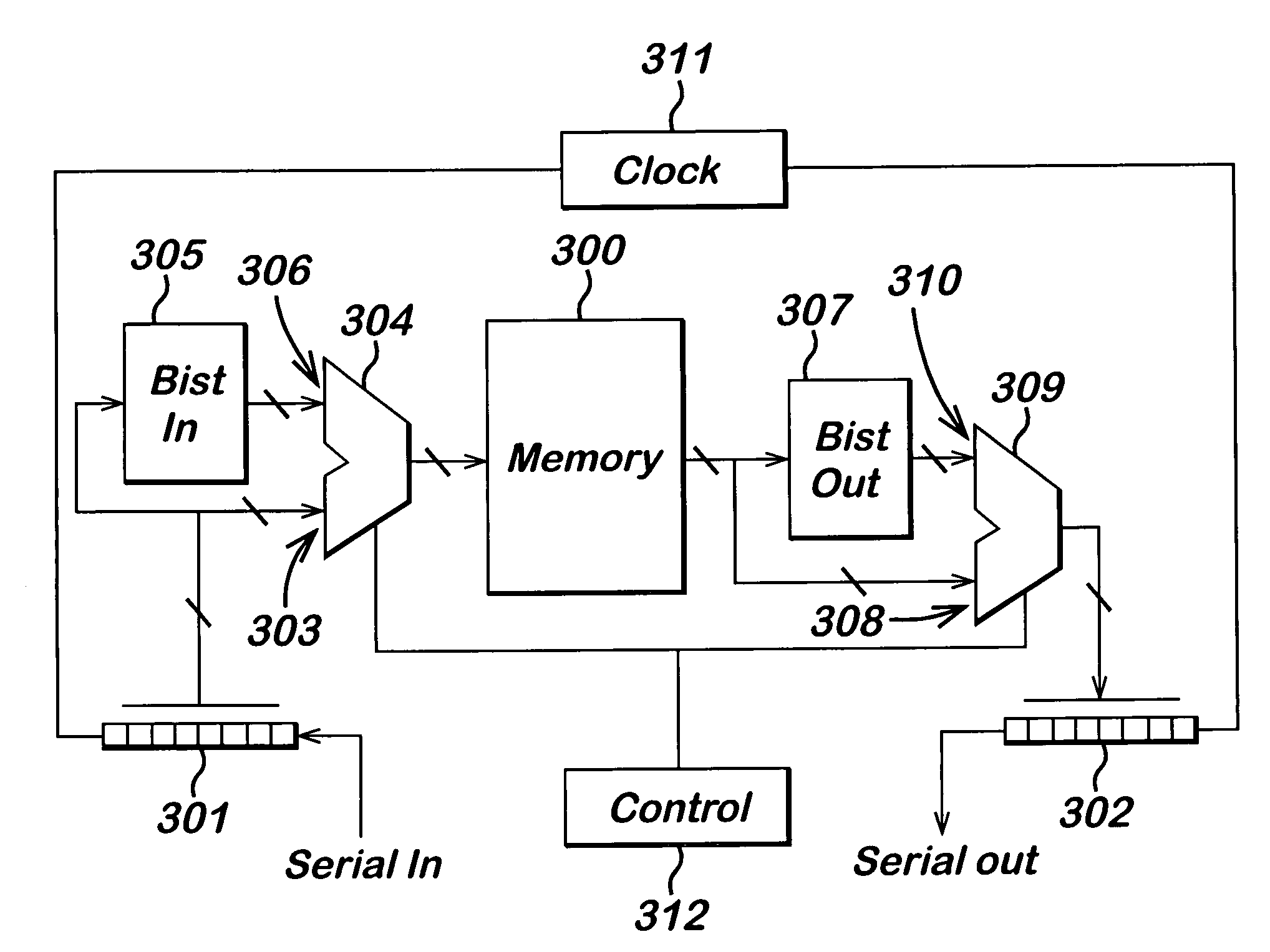
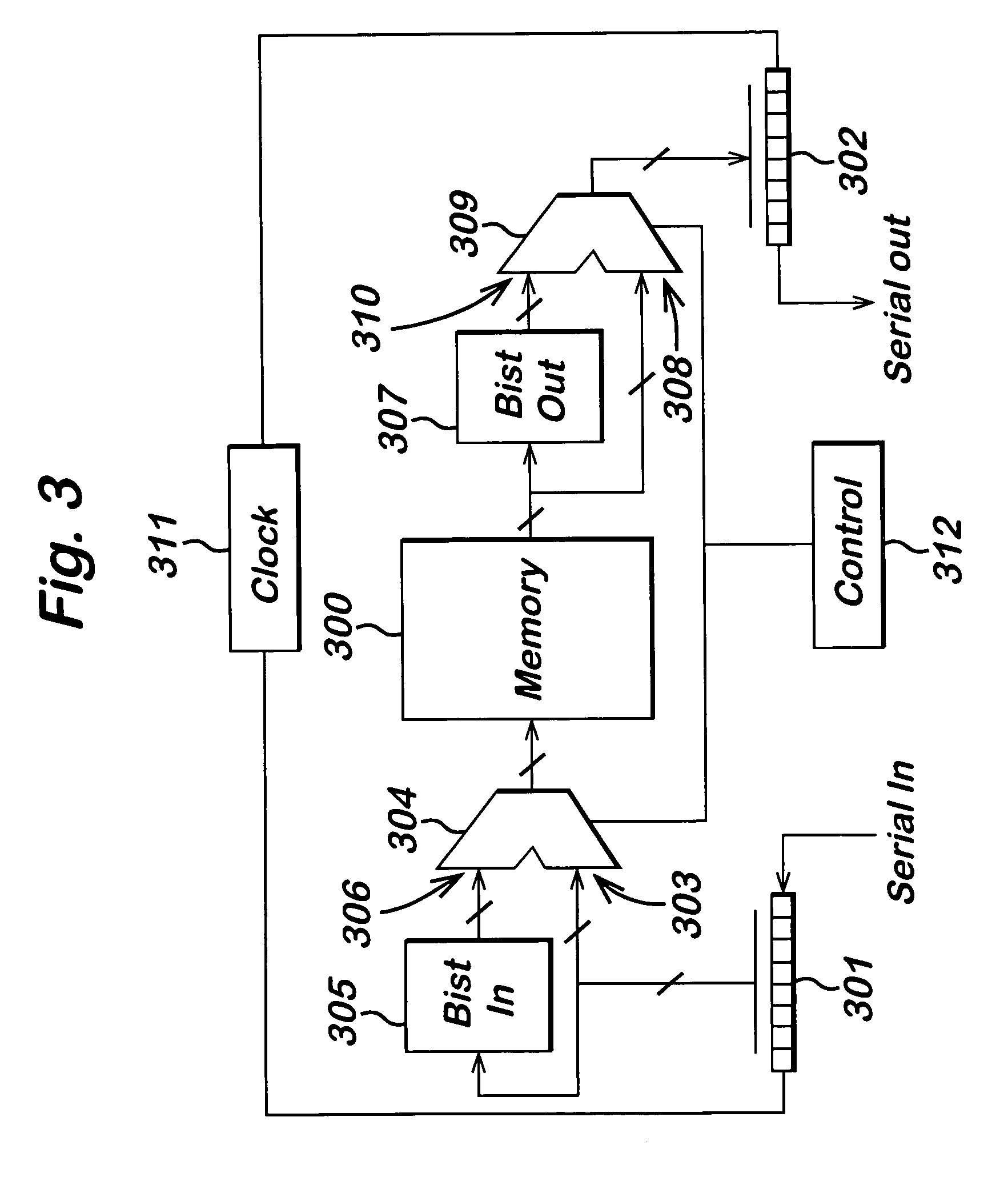
[0038]Referring to the FIG. 3, operative circuitry in the form of a block of memory 300 is provided with scan chains for input and output in the form of stimulus scan cells 301 and response scan cells 302. The stimulus scan cells accept serial input and provide a parallel output both to a first input 303 of a first multiplexor 304 and to the input of stimulus circuitry 305. The output of the stimulus circuitry 305 is provided to a second input 306 of the first multiplexor 304. The output of the first multiplexor 304 is connected to an input of the memory block 300.

[0039]An output of the memory block 300 is connected both to an input of capture circuitry 307 and to a first input 308 of a second multiplexor 309. The output of the second multiplexor 309 is connected to the input of the response scan cells, which are configured to clock data out serially.

[0040]Clock signals are provided to the various components from a clock generator 311, and control signals are provided by control cir...


PUM


Abstract

Test circuitry for testing an integrated circuit, the integrated circuit being configurable to accept input data from stimulus scan cells and to provide output data to response scan cells, the test circuitry including stimulus circuitry for providing test data to the integrated circuit; input selection means operable to control which of the test data and the input data are received at the integrated circuit; capture circuitry for capturing output data from the integrated circuit and generating response data; output selection means operable to select which of the output data and the response data are received by the response scan cells.

Description

FIELD OF INVENTION[0001]The present invention relates to testing of integrated circuits using built-in testing circuitry.[0002]The invention has been developed primarily for use in testing memory circuitry, and will be described hereinafter with reference to this application. However, it will be appreciated that the invention is not limited to this particular use and can be applied to many other types of integrated circuits having scan chains for data input and output.BACKGROUND TO INVENTION[0003]Presently, memory testing at integrated circuit level is usually handled in one of two ways. For relatively small memories (say, about 500 bytes or less), existing scan chains can be used. For example, referring to FIG. 1, data is fed serially into stimulus scan cells 10 until they contain the desired input values. The output of the stimulus scan cells 10 is then clocked into a memory location within memory block 11. The memory location is read out into response scan cells 12, and the outpu...

Claims


Application Information

Patent Timeline
Patent Type & Authority Patents(United States)
IPC IPC(8): G11C29/00G01R31/28G11C29/14G11C29/48
CPCG11C29/48G11C29/14
Inventor FIRTH, STEVENBARNES, WILLIAM BRYAN
Owner STMICROELECTRONICS LTD
Features
  • R&D
  • Intellectual Property
  • Life Sciences
  • Materials
  • Tech Scout
  • Unparalleled Data Quality
  • Higher Quality Content
  • 60% Fewer Hallucinations
Learn More