Phase change memory device employing thermal-electrical contacts with narrowing electrical current paths

a phase change memory and thermal-electrical contact technology, applied in the direction of bulk negative resistance effect devices, semiconductor devices, electrical equipment, etc., can solve the problems of slow reading and programming, large power consumption, and increasing the difficulty of cell size reduction, so as to reduce the volume of programmed phase change memory material and efficiently focus the generated heat

Inactive Publication Date: 2006-03-14
SILICON STORAGE TECHNOLOGY
View PDF9 Cites 65 Cited by
  • Summary
  • Abstract
  • Description
  • Claims
  • Application Information

AI Technical Summary

Benefits of technology

[0010]The present invention solves the aforementioned problems by providing a memory cell design that reduces the volume of the programmed phase change memory material, and efficiently focusing generated heat onto that volume of material using a narrowing current path.

Problems solved by technology

However, EEPROM memory cells are getting more difficult to scale down to smaller sizes, are relatively slow to read and program, and can consume a relatively large amount of power.
While this technique reduces the width of the memory material block immediately adjacent the heating electrode, it also results in the formation of the memory material block over just part of the heating electrode, which inefficiently transfers heat to the block of memory material using only part of the electrode's upper surface.
This technique also fails to reduce the overall width of the memory cell, as well as effectively reduce the depth of memory material being programmed.

Method used


Image

  • Phase change memory device employing thermal-electrical contacts with narrowing electrical current paths
  • Phase change memory device employing thermal-electrical contacts with narrowing electrical current paths
  • Phase change memory device employing thermal-electrical contacts with narrowing electrical current paths

Examples


Embodiment Construction

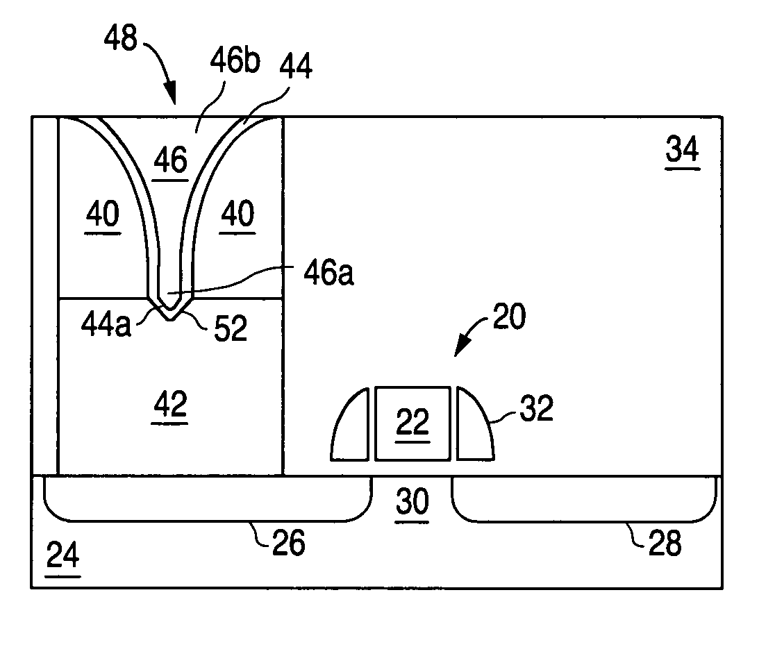
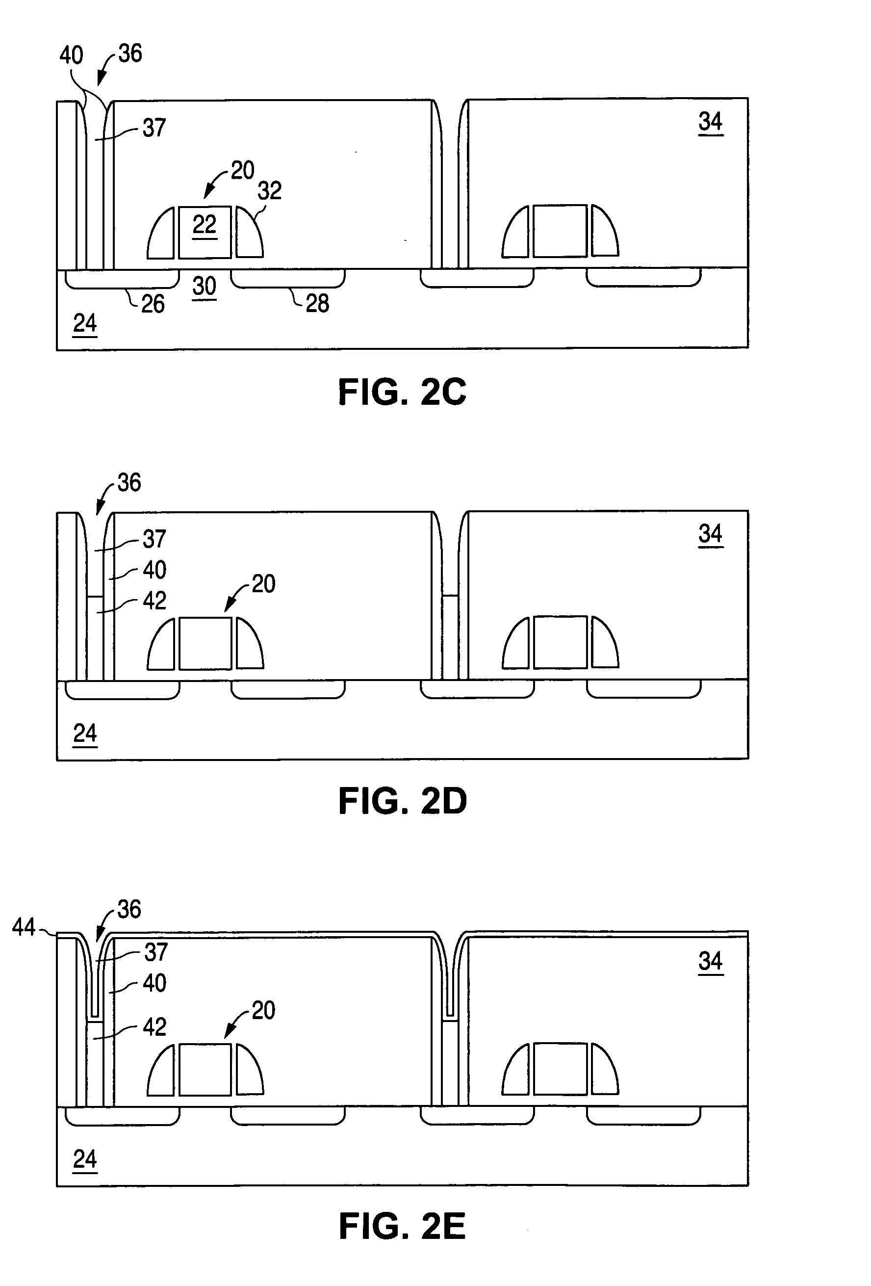
[0024]The present invention is an improved phase change memory device, and method of making such a device, where the volume of the phase change memory material programmed in the memory cell is reduced, and the heat used to program the memory device is efficiently focused onto that volume of material using a narrowing current path having a minimum cross-section adjacent that volume of material.

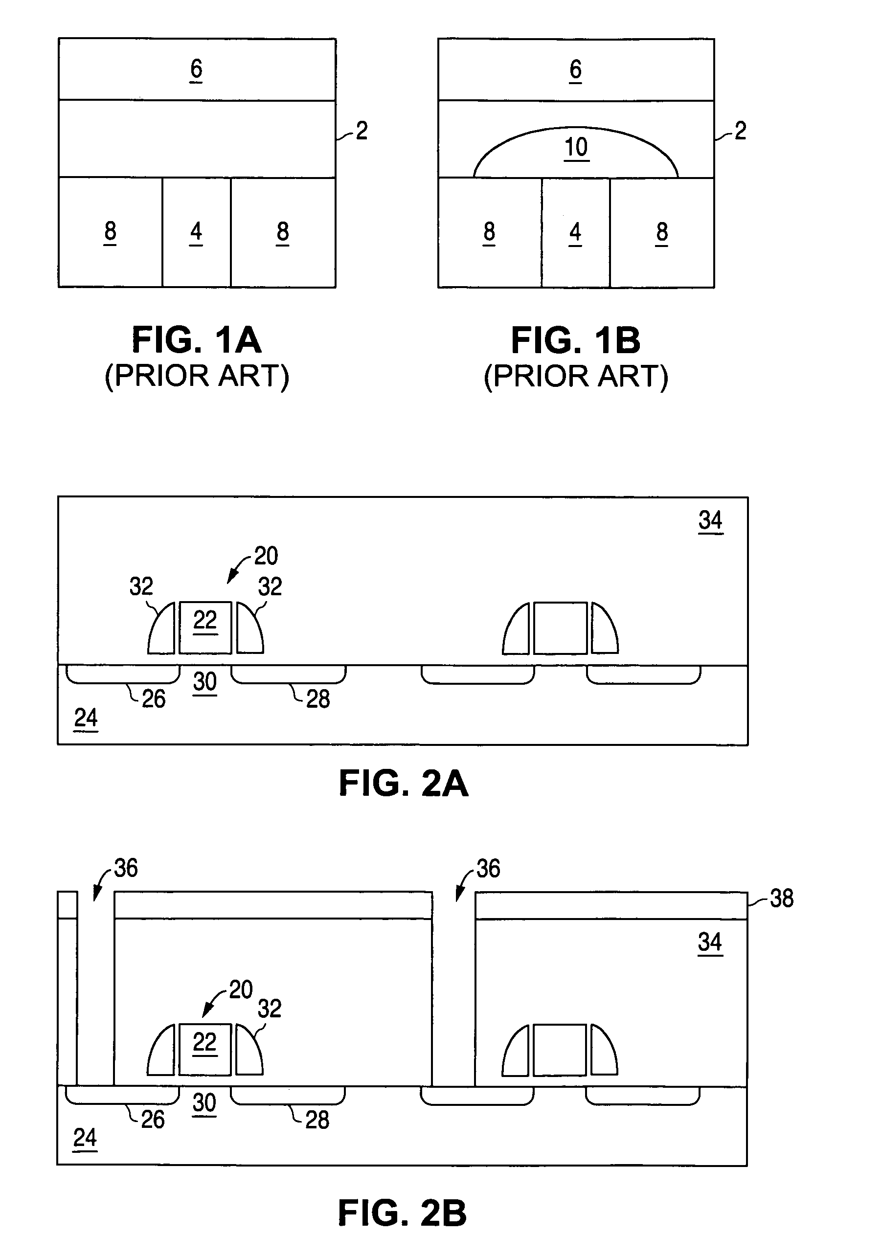
[0025]FIGS. 2A to 2F illustrate the formation of the phase change memory cells of the present invention. FIG. 1A illustrates well known MOS FET transistors 20, the formation of which is well known in the art and not described herein in any detail. The MOS FET transistors 20 each include a conductive gate 22 formed over and insulated from a silicon substrate 24. Source and drain regions 26 / 28 (i.e. first and second regions that are interchangeable) are formed in the substrate 24 and have a conductivity type (e.g. N type) different from that of the substrate 24 (e.g. P type). The channel region 3...


PUM


Abstract

A phase changing memory device, and method of making the same, that includes contact holes formed in insulation material that extend down to and exposes source regions for adjacent FET transistors. Spacer material is disposed in the holes with surfaces that define openings each having a width that narrows along a depth of the opening. Lower electrodes are disposed in the holes. A layer of phase change memory material is disposed along the spacer material surfaces and along at least a portion of the lower electrodes. Upper electrodes are formed in the openings and on the phase change memory material layer. For each contact hole, the upper electrode and phase change memory material layer form an electrical current path that narrows in width as the current path approaches the lower electrode, such that electrical current passing through the current path generates heat for heating the phase change memory material disposed between the upper and lower electrodes.

Description

FIELD OF THE INVENTION[0001]The present invention relates to phase change memory devices, and more particularly to phase change memory devices employing narrowing electrical current paths for focusing the application of heat onto selected portions of phase change memory material.BACKGROUND OF THE INVENTION[0002]There are many types of computer memory technologies that are presently used to store computer programs and data, including dynamic random access memory (DRAM), static random access memory (SRAM), erasable programmable read-only memory (EPROM), and electrically erasable programmable read only memory (EEPROM), etc. Some memory technologies require electrical power to maintain the stored data (i.e. volatile memory), while others do not (i.e. non-volatile memory). Memory technologies can be read only, write once only, or repeatedly read / write.[0003]There is an increasing demand for repeatedly read / write, non-volatile memory. The primary non-volatile memory technology presently u...

Claims


Application Information

Patent Timeline
Patent Type & Authority Patents(United States)
IPC IPC(8): H01L47/00H01L27/24H01L45/00
CPCH01L27/2436H01L45/06H01L45/1233H01L45/1666H01L45/1273H01L45/144H01L45/126H10B63/30H10N70/231H10N70/826H10N70/8413H10N70/8418H10N70/8828H10N70/061
Inventor CHEN, BOMY
Owner SILICON STORAGE TECHNOLOGY
Why Eureka
Try Eureka