Non-volatile memory device

a memory device and non-volatile technology, applied in semiconductor devices, semiconductor/solid-state device details, electrical devices, etc., can solve the problems of single-electron memory devices that require low operating temperatures, poor data retention of silicon nanocrystal-based memory devices, and considerable drawbacks associated with their practical application, etc., to achieve good charge retention and small design features

Inactive Publication Date: 2006-03-14
MONTEREY RES LLC
View PDF5 Cites 86 Cited by
  • Summary
  • Abstract
  • Description
  • Claims
  • Application Information

AI Technical Summary

Benefits of technology

[0004]There exists a need for a memory device with small design features that exhibits good charge retention at normal room temperature ranges.
[0005]These and other needs are met by the present invention, where a non-volatile memory device is formed using a quantum well as a floating gate. The resulting memory device is able to achieve good charge retention at room temperature.

Problems solved by technology

Such devices, however, have considerable drawbacks associated with their practical application.
For example, single-electron memory devices require low operating temperatures and silicon nanocrystal-based memory devices exhibit poor data retention.

Method used


Image

  • Non-volatile memory device
  • Non-volatile memory device
  • Non-volatile memory device

Examples


Embodiment Construction

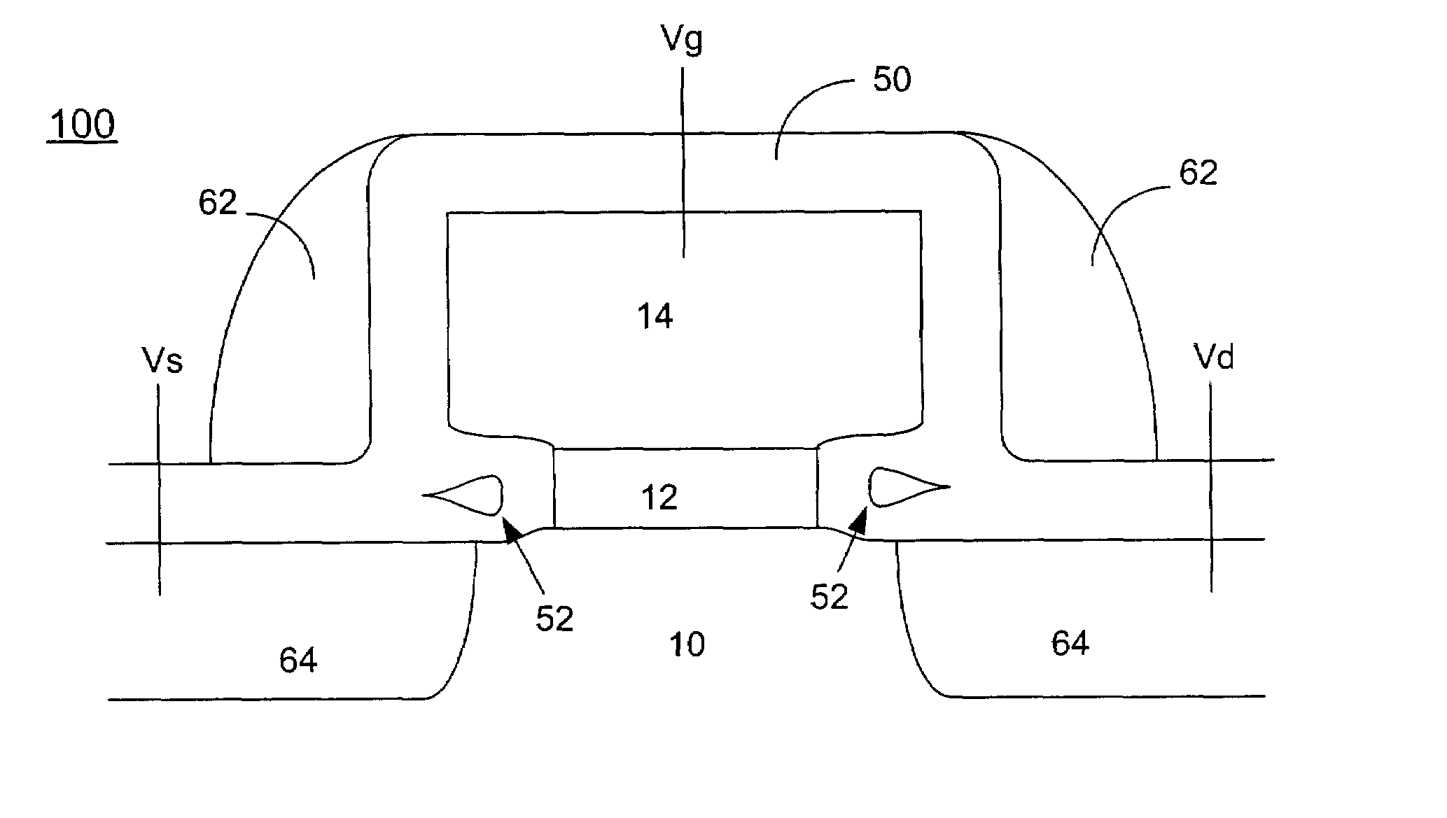
[0023]The present invention addresses constraints associated with non-volatile memory devices having small design features by using a quantum well as a floating gate electrode for a memory device. The resulting memory device can be scaled well below a 5 nanometer (nm) gate length and exhibits good charge retention at room temperature.

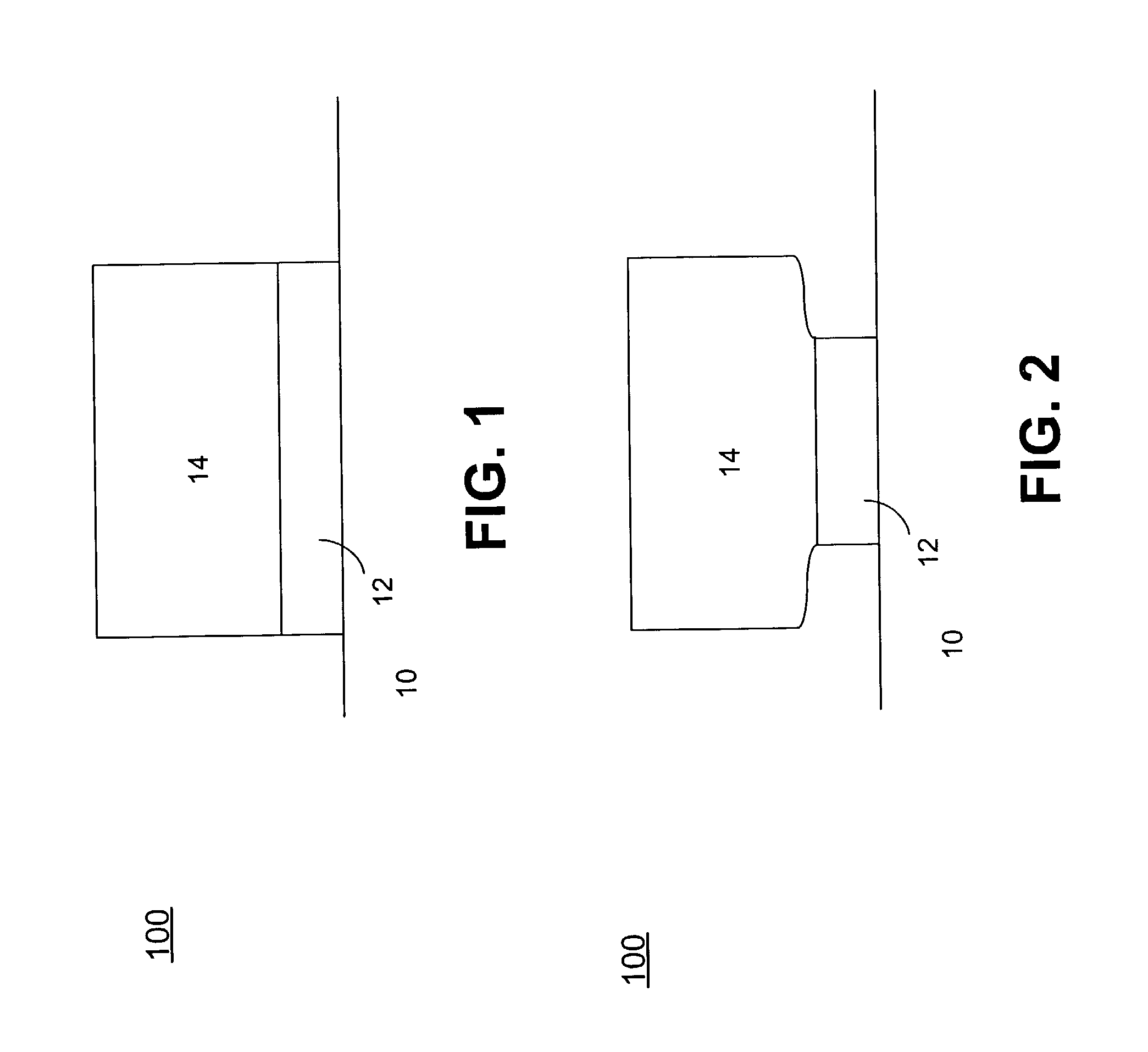
[0024]FIG. 1 illustrates the cross-section of a semiconductor device 100 formed in accordance with an embodiment of the present invention. Substrate 10, consistent with the present invention, comprises doped monocrystalline silicon. In an exemplary implementation, substrate 10 may be doped with p-type impurities. For example, a p-type impurity, such as boron, may be implanted at a dosage of about 5×10¹² atoms / cm2 to about 5×10¹³ atoms / cm2 and an implantation energy of about 0–20 KeV to dope substrate 10.

[0025]A dielectric layer, such as gate oxide 12, may then be formed on semiconductor substrate 10. For example, gate oxide 12 may be grown to a thicknes...


PUM


Abstract

A non-volatile memory device is provided by forming a tunnel oxide layer and a gate electrode on the tunnel oxide layer. Silicon structures are formed below the side surfaces of the gate electrode and act as a floating gate electrode for the non-volatile memory device.

Description

RELATED APPLICATION[0001]This application claims priority under 35 U.S.C. § 119 based on U.S. Provisional Application No. 60 / 390,116, filed Jun. 21, 2002, the disclosure of which is incorporated herein by reference.TECHNICAL FIELD[0002]The present invention relates generally to memory devices and, more particularly, to non-volatile memory devices.BACKGROUND ART[0003]Non-volatile memory devices that use a small number of electrons to store data have been recently demonstrated. Such devices, however, have considerable drawbacks associated with their practical application. For example, single-electron memory devices require low operating temperatures and silicon nanocrystal-based memory devices exhibit poor data retention.DISCLOSURE OF THE INVENTION[0004]There exists a need for a memory device with small design features that exhibits good charge retention at normal room temperature ranges.[0005]These and other needs are met by the present invention, where a non-volatile memory device i...

Claims


Application Information

Patent Timeline
Patent Type & Authority Patents(United States)
IPC IPC(8): H01L29/788H01L29/80H01L21/28H01L27/115H01L29/423H01L29/49H01L29/78H01L29/786
CPCH01L21/28273H01L27/115H01L29/42332H01L29/7883H01L29/4983H01L29/7831H01L29/78645H01L29/42384H01L29/40114H10B69/00
Inventor KRIVOKAPIC, ZORAN
Owner MONTEREY RES LLC
Why Eureka
Try Eureka