Programmable logic device (PLD)

a logic device and programmable logic technology, applied in the field of semiconductor devices, can solve the problems of leakage current through gate insulating films, deterioration of charge retention characteristics of nodes, etc., and achieve the effects of preventing an increase in the area occupied by memory cells, excellent charge retention characteristics, and high area efficiency

Inactive Publication Date: 2017-09-12
SEMICON ENERGY LAB CO LTD
View PDF162 Cites 4 Cited by
  • Summary
  • Abstract
  • Description
  • Claims
  • Application Information

AI Technical Summary

Benefits of technology

[0010]Miniaturization of Si transistors progresses with shrinking design rules. Reduction in the size of elements results in thinner gate insulating films, thereby posing a problem of leakage current through a gate insulating film.
[0014]Another object of one embodiment of the present invention is to provide a novel-structured semiconductor device with excellent charge retention characteristics of a node that holds charge. Another object of one embodiment of the present invention is to provide a novel-structured semiconductor device in which a function of a nonvolatile memory circuit is not impaired even when leakage current through a gate insulating film of a Si transistor occurs. Another object of one embodiment of the present invention is to provide a novel-structured semiconductor device that has high area efficiency by preventing an increase in area occupied by memory cells due to the increase in the number of components.
[0017]With the above structure, charge at the node for holding charge is held in the nonvolatile memory circuit included in a programmable switch element; thus, the function of the nonvolatile memory circuit can be maintained. Moreover, it is possible to achieve a programmable logic device in which a function of the path transistor in the programmable switch element is not impaired even if leakage current occurs in the Si transistor because of miniaturization.
[0019]With the above structure, even if leakage current occurs in the Si transistor because of miniaturization, charge retention characteristics of the node that holds charge are improved, and the function of a nonvolatile memory circuit with excellent charge retention characteristics is maintained. Furthermore, stacking transistors composing a memory cell prevents the increase in the memory cell area due to the increase in the number of elements.
[0040]One embodiment of the present invention can provide a novel-structured programmable logic device in which a function of a programmable switch element as a nonvolatile memory circuit is not impaired. Moreover, one embodiment of the present invention can provide a novel-structured programmable logic device in which a function of a nonvolatile memory circuit in a programmable switch element is not impaired even when leakage current through a gate insulating film of a Si transistor serving as a path transistor occurs.
[0041]One embodiment of the present invention can provide a novel-structured semiconductor device with excellent charge retention characteristics of a node that holds charge. One embodiment of the present invention can provide a novel-structured semiconductor device in which a function of a nonvolatile memory circuit is not impaired even when leakage current through a gate insulating film of a Si transistor occurs. Further, one embodiment of the present invention can provide a novel-structured semiconductor device that has high area efficiency by preventing an increase in area occupied by memory cells due to the increase in the number of components.

Problems solved by technology

Reduction in the size of elements results in thinner gate insulating films, thereby posing a problem of leakage current through a gate insulating film.
Thus, charge retention characteristics of the node deteriorate even when the off-state leakage current of the OS transistor (off-state current) is low.

Method used


Image

  • Programmable logic device (PLD)
  • Programmable logic device (PLD)
  • Programmable logic device (PLD)

Examples


embodiment 1

[0083]In this embodiment, a structure of a programmable switch element will be described.

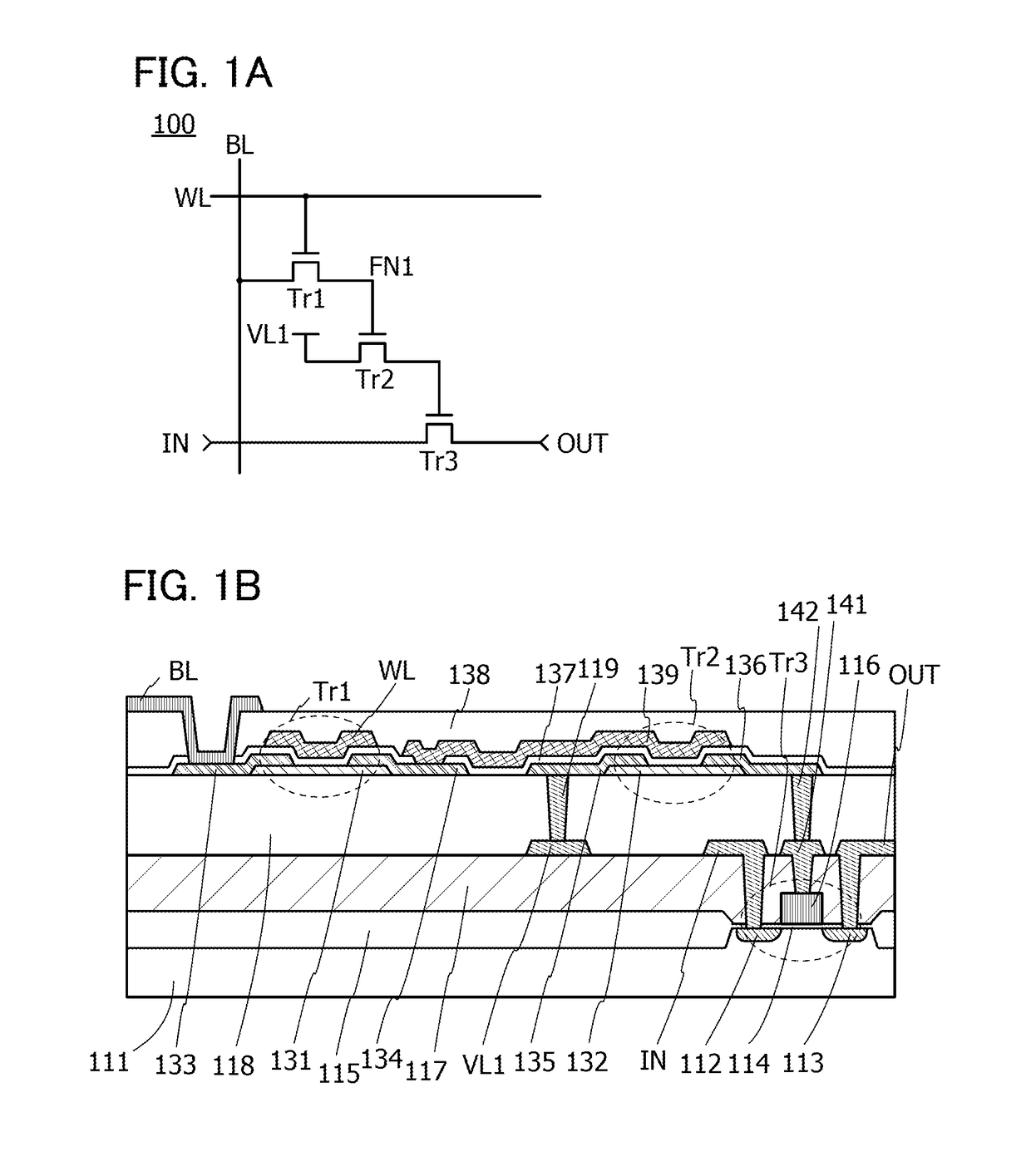
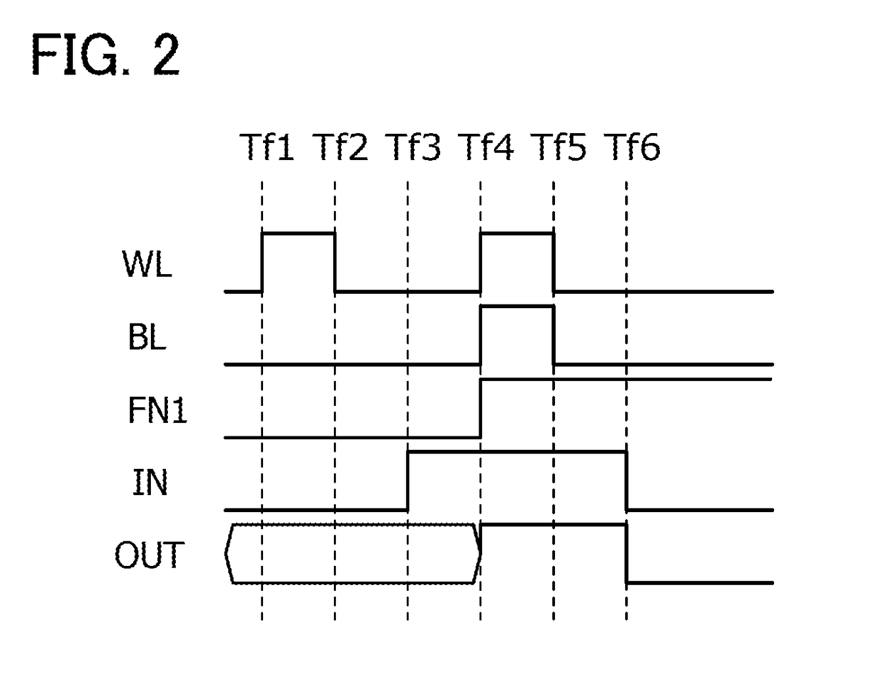
[0084]FIG. 1A is a circuit diagram illustrating the structure of a programmable switch element. FIG. 1B is a cross-sectional schematic view corresponding to the circuit diagram.

[0085]A programmable switch element 100 illustrated in FIG. 1A includes a transistor Tr1, a transistor Tr2, and a transistor Tr3. Note that the transistors Tr1 to Tr3 are n-channel transistors in FIG. 1A.

[0086]The transistor Tr1 has a function of controlling writing of configuration data into the programmable switch element 100 in accordance with a word signal. A gate of the transistor Tr1 is connected to a word line WL for applying a word signal (wiring). One of a source and a drain of the transistor Tr1 is connected to a bit line BL for applying configuration data (wiring).

[0087]The transistor Tr2 has a function of controlling the on / off state of the transistor Tr3 in accordance with configuration data written into the ...

embodiment 2

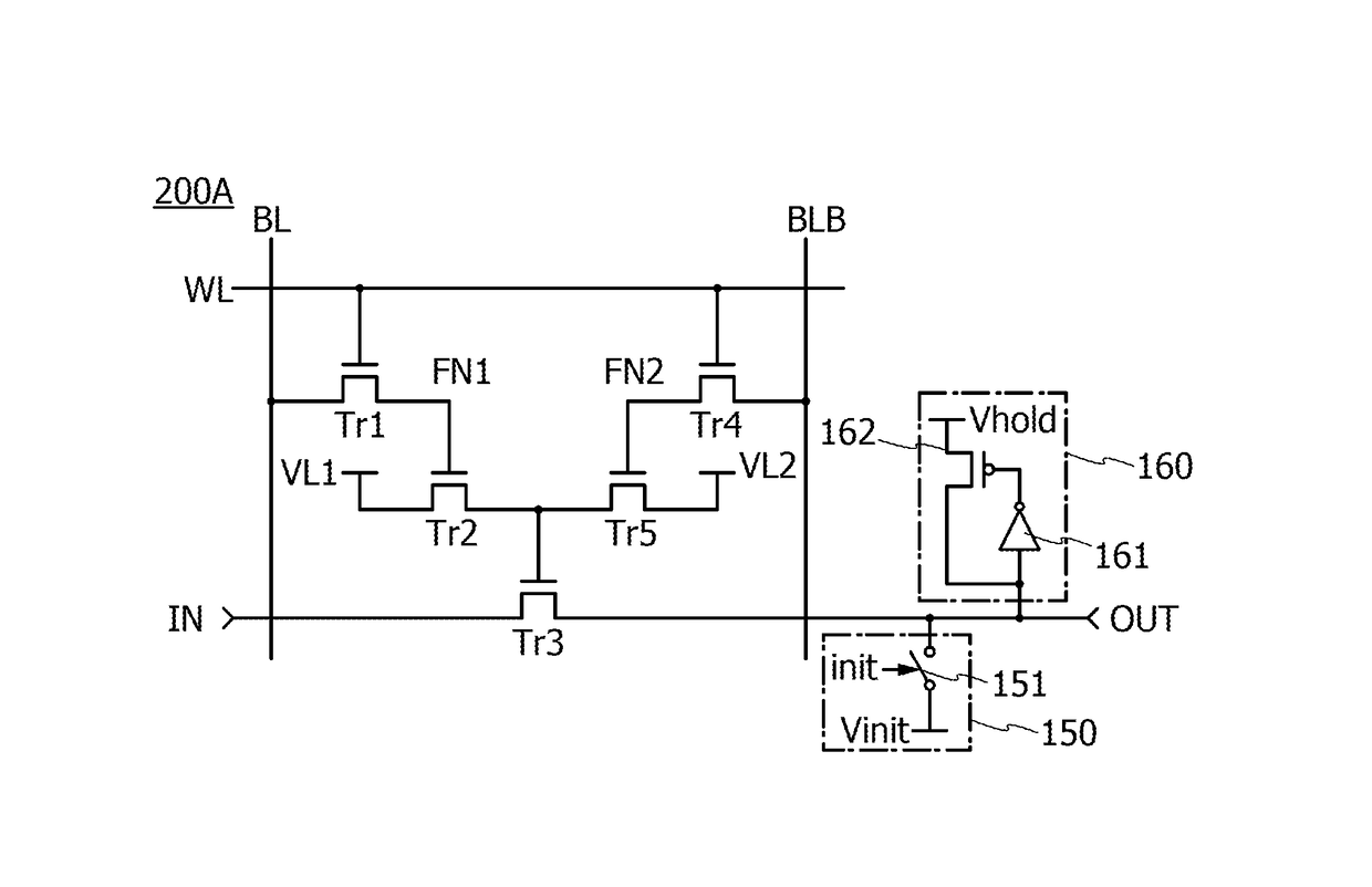
[0151]In this embodiment, a structure of a programmable switch element different from those in Embodiment 1 will be described.

[0152]FIG. 6A is a circuit diagram illustrating the structure of a programmable switch element. FIG. 6B is a cross-sectional schematic view corresponding to the circuit diagram. Note that in this embodiment, components common to Embodiment 1 are denoted by the same reference numerals and the description is omitted in some cases.

[0153]A programmable switch element 200A illustrated in FIG. 6A includes the transistor Tr1, the transistor Tr2, the transistor Tr3, a transistor Tr4, and a transistor Tr5. Note that the transistors Tr1 to Tr5 are n-channel transistors in FIG. 6A. The circuit diagram in FIG. 6A of this embodiment illustrates a structure where the transistors Tr4 and Tr5 are added to the structure in FIG. 1A of Embodiment 1.

[0154]As in FIG. 1A of Embodiment 1, the transistor Tr1 has a function of controlling writing of configuration data into the progra...

embodiment 3

[0214]This embodiment will show a structure example of a PLD, a structure example of a programmable logic element, and a layout example of circuits included in a PLD.

[0215]FIG. 11A illustrates an example of a programmable logic element (PLE) 40. The programmable logic element 40 illustrated in FIG. 11A includes a look-up table (LUT) 41, a flip-flop (FF) 42, and a configuration memory (CM) 43. Logical operation of the LUT 41 is determined in accordance with configuration data in the configuration memory 43. Specifically, one output value of the LUT 41 with respect to input values of a plurality of input signals supplied to input terminals 44 is determined. Then, the LUT 41 outputs a signal including the output value. The flip-flop 42 holds the signal output from the LUT 42 and outputs an output signal corresponding to the signal from a first output terminal 45 and a second output terminal 46 in synchronization with a clock signal CLK.

[0216]Note that the programmable logic element 40 ...


PUM


Abstract

To provide a semiconductor device with excellent charge retention characteristics, a transistor including a thick gate insulating film to achieve low leakage current is additionally provided such that its gate is connected to a node for holding charge. The node is composed of this additional transistor and a transistor using an oxide semiconductor in its semiconductor layer including a channel formation region. Charge corresponding to data is held at the node.

Description

BACKGROUND OF THE INVENTION[0001]1. Field of the Invention[0002]The present invention relates to semiconductor devices, and particularly to a programmable logic device and a semiconductor device that can change a hardware configuration.[0003]2. Description of the Related Art[0004]A programmable logic device (PLD) includes a plurality of programmable logic elements and a plurality of programmable switch elements. A circuit structure of a PLD can be varied to change its function in such a manner that a function of each programmable logic element or a connection between programmable logic elements through programmable switch elements is changed by programming performed by a user after fabrication.[0005]A function of each programmable logic element and a connection between programmable logic elements through programmable switch elements are determined by configuration data. Configuration data is stored in a memory circuit included in a programmable logic element or a memory circuit incl...

Claims


Application Information

Patent Timeline
Patent Type & Authority Patents(United States)
IPC IPC(8): H01L27/115H01L27/11529H01L27/11558H01L27/12H01L27/07H01L27/088H01L27/06
CPCH01L27/11529H01L27/11558H01L27/0623H01L27/0705H01L27/088H01L27/1225H10B41/60H01L29/78606H01L29/78645H01L29/78696H10B41/41
Inventor KUROKAWA, YOSHIYUKI
Owner SEMICON ENERGY LAB CO LTD
Why Eureka
Try Eureka