Non-volatile memory structure and method for preparing the same

a non-volatile memory and structure technology, applied in the direction of basic electric elements, electrical equipment, semiconductor devices, etc., can solve the problem that the electric charge in the floating gate may be completely lost, and achieve the effect of improving the endurance of charge retention

Inactive Publication Date: 2009-11-19
PROMOS TECH INC
View PDF4 Cites 6 Cited by
  • Summary
  • Abstract
  • Description
  • Claims
  • Application Information

AI Technical Summary

Benefits of technology

[0009]The metallic nano-dots are isolated from each other by the silicon-oxy-nitride layer, and the charge leakage of one metallic nano-dot will not influence the trapped electric charge of the other metallic nano-dots. Consequently, the electric charges trapped in the metallic nano-dots, serving as discrete floating gates, will not be completely lost even if there is a leakage path between one of the metallic nano-dots and another conductive member of the non-volatile memory structure. In other words, the charge-trapping structure with embedded metallic nano-dots isolated from each other by the silicon-oxy-nitride layer can provide better charge retention endurance than the conventional floating gate made of a single conductive block.

Problems solved by technology

However, the trapped electric charges in the floating gate may be completely lost if there is a leakage path between the floating gate and another conductive member of the floating gate flash memory.

Method used


Image

  • Non-volatile memory structure and method for preparing the same
  • Non-volatile memory structure and method for preparing the same
  • Non-volatile memory structure and method for preparing the same

Examples


Embodiment Construction

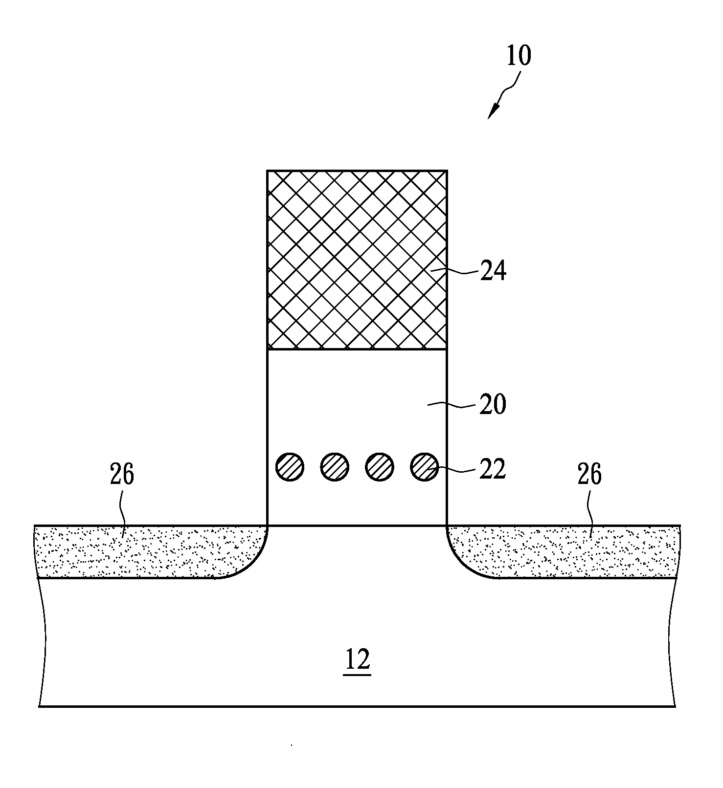
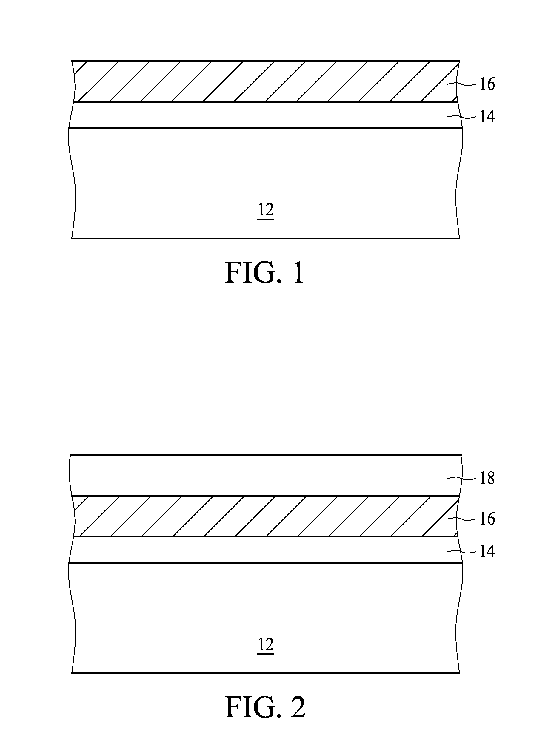
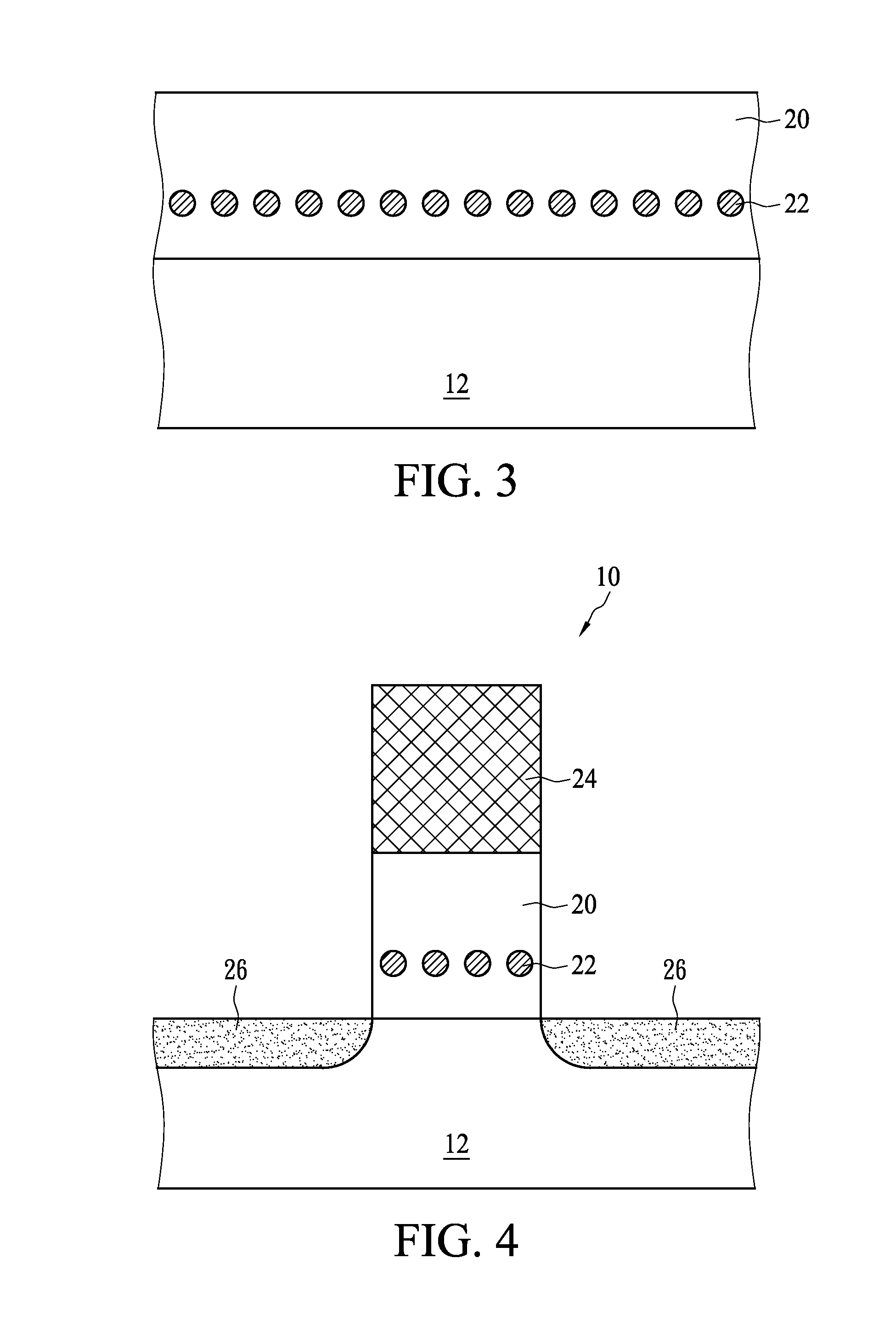
[0016]FIG. 1 to FIG. 4 illustrate a method for preparing a non-volatile memory structure 10 according to one embodiment of the present invention. Referring to FIG. 1, a high-k dielectric layer 14 is formed on a silicon substrate 12 by a first thermal oxidation process, and a metal-containing semiconductor layer 16 is then formed on the high-k dielectric layer 14 by a chemical vapor phase deposition process. The high-k dielectric layer 14 is made of high-k material with a dielectric constant higher than the dielectric constant of the silicon, and can be a silicon oxide layer. The metal-containing semiconductor layer 16 may include silicon or germanium, and can be metallic silicide layer such as tungsten silicide (WSix) layer, a cobalt silicide (CoSix) layer, or a titanium silicide (TiSix) layer.

[0017]The first thermal oxidation process can be performed at a temperature between 950 and 1200° C. for 20 to 1200 seconds, preferably for 30 to 80 seconds. In particular, the first thermal o...


PUM


Abstract

A non-volatile memory structure includes a substrate having two doped regions, a charge-trapping structure positioned substantially between the two doped regions, and a conductive structure positioned on the charge-trapping structure, wherein the charge-trapping structure includes a silicon-oxy-nitride layer and metallic nano-dots embedded in the silicon-oxy-nitride layer. The non-volatile memory structure formed by performing a first thermal oxidation process to form a high-k dielectric layer on a substrate, forming a metal-containing semiconductor layer including silicon or germanium on the high-k dielectric layer, forming a silicon layer on the metal-containing semiconductor layer, and performing a second thermal oxidation process to convert the metal-containing semiconductor layer to a silicon-oxy-nitride layer with embedded metallic nano-dots, wherein at least one of the first thermal oxidation process and the second thermal oxidation process is performed in a nitrogen-containing atmosphere.

Description

BACKGROUND OF THE INVENTION[0001](A) Field of the Invention[0002]The present invention relates to a non-volatile memory structure and method for preparing the same, and more particularly, to a non-volatile memory structure with high-density metallic nano-dots and method for preparing the same.[0003](B) Description of the Related Art[0004]Non-volatile memories such as flash memory have been widely used for data storage in digital products such as laptop computers, personal digital assistants, cell phones, digital cameras, digital recorders, and MP3 players. Non-volatile memory devices that use charge-trapping mechanisms have been widely studied. Advantages of flash memories include non-volatility, i.e., information can be stored in the memory even when power supply is disconnected, and fast erasure speed.[0005]A trapping-type non-volatile memory device such as floating gate flash memory can be manufactured on a semiconductor substrate and generally includes an array of memory cells e...

Claims


Application Information

Patent Timeline
Patent Type & Authority Applications(United States)
IPC IPC(8): H01L29/792H01L21/28
CPCH01L29/7881H01L29/42332
Inventor HSIEH, WAN TENGLIAO, I HSUANCHEN, SHIH FANGCHANG, TING CHANGXI, PENG BOCHEN, WEI REN
Owner PROMOS TECH INC
Why Eureka
Try Eureka