Semiconductor device having nonvolatile memory device with improved charge holding property

a nonvolatile memory and semiconductor technology, applied in semiconductor devices, electrical devices, transistors, etc., can solve the problems of deterioration of charge holding properties, inability to provide the first interlayer insulating layer, and more problems owing to excessive etching, etc., to achieve excellent charge holding properties

Inactive Publication Date: 2009-01-06
SEIKO EPSON CORP
View PDF12 Cites 4 Cited by
  • Summary
  • Abstract
  • Description
  • Claims
  • Application Information

AI Technical Summary

Benefits of technology

[0008]An advantage of some aspects of the invention is to provide a semiconductor device, which is microminiaturized and has a nonvolatile memory with an excellent charge holding property.

Problems solved by technology

However, when forming an etching stopper film on a nonvolatile memory having a floating gate electrode which is an example of a semiconductor element, depending on a material of the etching stopper film, deterioration of a charge holding property may occur.
However, the first interlayer insulating layer is not provided above the nonvolatile memory.
Especially, the more the semiconductor device is subjected to microminiaturization, the more problem due to excessive etching tends to occur.
When the etching stopper film having the charge supplementary property is placed above the floating gate electrode, an electron which is written is lost, so that data may be lost.

Method used


Image

  • Semiconductor device having nonvolatile memory device with improved charge holding property
  • Semiconductor device having nonvolatile memory device with improved charge holding property
  • Semiconductor device having nonvolatile memory device with improved charge holding property

Examples


Embodiment Construction

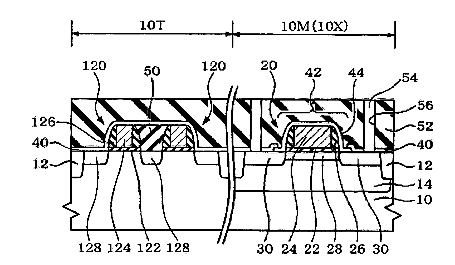
[0048]Embodiments of the invention will be described below with reference to the drawings.

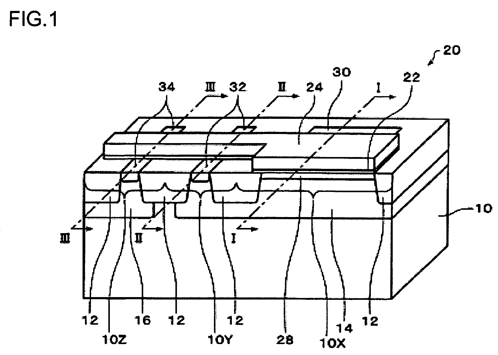
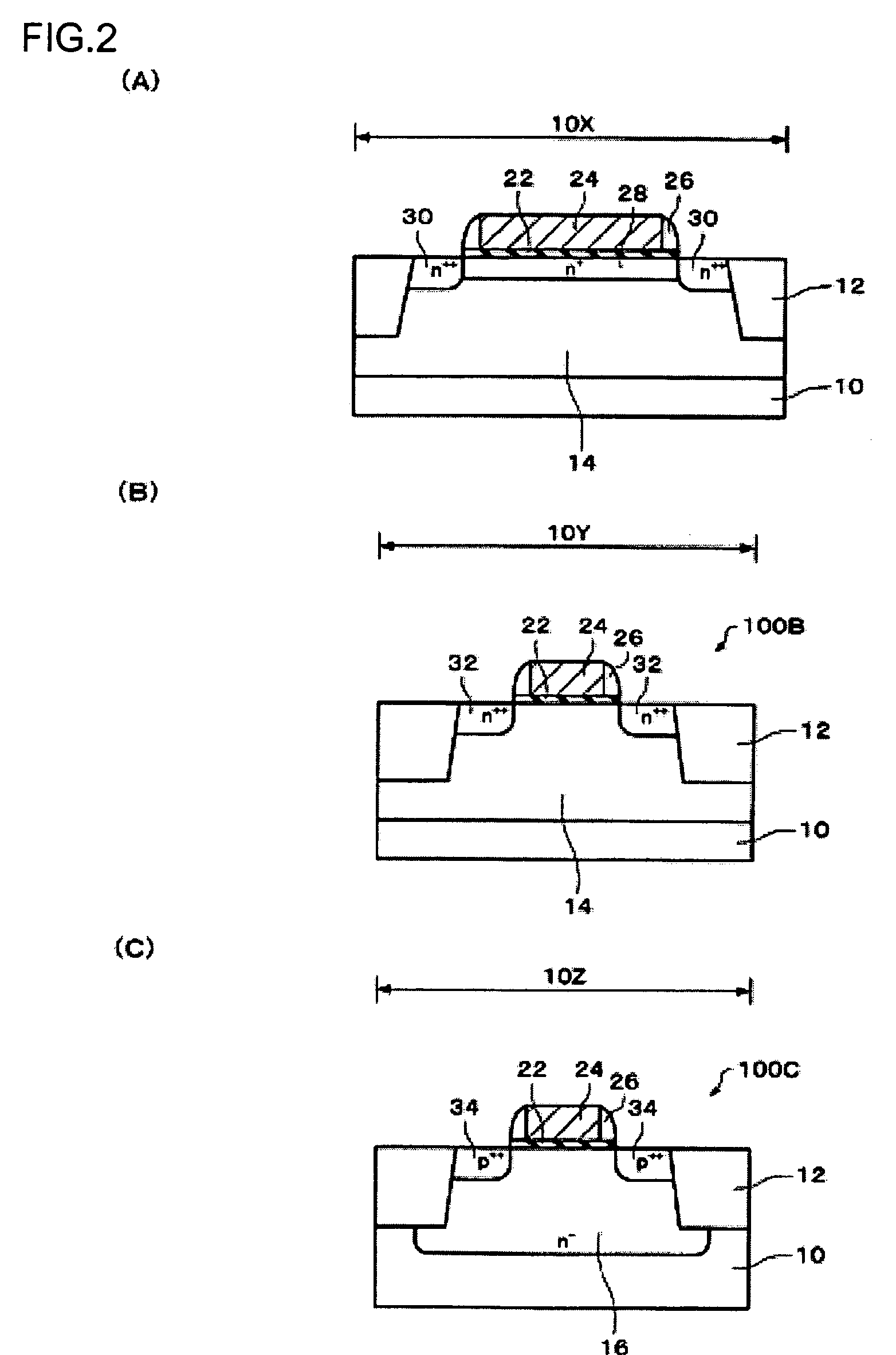
[0049]1. First, a nonvolatile memory (hereinafter may be referred to as the “memory cell” as well) 20 which is included in a semiconductor device according to the embodiment will be described while referring to FIGS. 1 and 2.

[0050]The memory cell 20 included in the semiconductor device of the embodiment is such that its control gate is an n-type impurity area inside a semiconductor layer 10, while its floating gate consists of a conductive layer of a one-layer polysilicon layer and the like (hereinafter referred to as the “nonvolatile memory device of one-layer type”).

[0051]FIG. 1 is a perspective view showing the memory cell, FIG. 2A is a sectional view along line I-I of FIG. 1, FIG. 2B is a sectional view along line II-II of FIG. 1, and FIG. 2C is a sectional view along line III-III of FIG. 1.

[0052]As shown in FIG. 1, the memory cell 20 in the embodiment is provided on a p-type semiconductor ...


PUM


Abstract

A semiconductor device includes: a semiconductor layer; a first area and a second area which are demarcated by a separation insulating layer provided on the semiconductor layer; a nonvolatile memory provided on the first area; a plurality of MOS transistors provided on the second area; a first interlayer insulating layer embedded between the plurality of MOS transistors on the second area; and a second interlayer insulating layer provided above the first area and the second area. The second interlayer insulating layer is provided as if covering the nonvolatile memory on the first area and, on the second area, provided, being above the first interlayer insulating layer, as if covering the MOS transistor.

Description

BACKGROUND OF THE INVENTION[0001]The entire disclosure of Japanese Patent Application No. 2005-027962, filed Feb. 3, 2005 is expressly incorporated by reference herein.[0002]1. Technical Field[0003]The invention relates to a semiconductor device.[0004]2. Related Art[0005]With recent trends for higher integration and microminiaturization of semiconductor devices, higher accuracy is being called for in alignment when forming a contact layer and the like connecting wiring to a semiconductor layer. Consequently, in JP-A-8-181204, there is disclosed a technique in which an etching stopper film is provided between an interlayer insulating layer and a semiconductor layer, whereby an element and a semiconductor layer will not suffer any damage even if excessive etching is carried out when forming a contact hole.[0006]JPA-8-181204 is an example of related art.[0007]However, when forming an etching stopper film on a nonvolatile memory having a floating gate electrode which is an example of a ...

Claims


Application Information

Patent Timeline
Patent Type & Authority Patents(United States)
IPC IPC(8): H01L29/94
CPCH01L27/105H01L27/11521H01L27/11526H01L27/11541H01L27/11543H01L27/11558H10B41/47H10B41/48H10B41/30H10B41/60H10B41/40
Inventor MARUO, YUTAKAINOUE, SUSUMUTAKEDA, YO
Owner SEIKO EPSON CORP
Why Eureka
Try Eureka