Fingerprint sensor using a piezoelectric membrane

a piezoelectric membrane and fingerprint sensor technology, applied in the direction of person identification, instruments, generators/motors, etc., can solve the problems of difficult to manufacture the fingerprint sensor as a one-chip type, difficult to precisely measure information, and difficult to achieve the effect of simple applications to portable systems

Active Publication Date: 2006-03-14
SAMSUNG ELECTRONICS CO LTD
View PDF7 Cites 25 Cited by
  • Summary
  • Abstract
  • Description
  • Claims
  • Application Information

AI Technical Summary

Benefits of technology

[0009]In an effort to solve the problems described above, it is a feature of an embodiment of the present invention to provide a fingerprint sensor in which: the fingerprint sensor has a membrane shape in which unit devices are arrayed, wherein the unit devices exploit a piezoelectric phenomenon to precisely sense information from a fingerprint, i.e., pressure from protrusions of the fingerprint and grooves between the protrusions of the fingerprint; capacitance measured based on changes in temperature and humidity are regular; and reliable results are obtained in-situ.

Problems solved by technology

As a result, security of one's private information has become a critical issue, and an individual fingerprint sensor is needed to protect an individual's information.
However, since information is read using a thick film and not a membrane, it is difficult to precisely measure information and to manufacture the fingerprint sensor as a one-chip type.
Accordingly, there is a problem in that it is difficult for an individual to carry the fingerprint sensor, and therefore simple applications to portable systems are difficult.
However, this way is very sensitive to temperature and moisture.
Additionally, there are problems in that additional circuitry and materials are necessary because of static electricity and it is difficult to draw regular results.
Moreover, the quantity of charge readable from the fingerprint and sensor surfaces when operating the fingerprint sensor is small and thus must be separately stored by repeatedly toggling a switch on and off.

Method used


Image

  • Fingerprint sensor using a piezoelectric membrane
  • Fingerprint sensor using a piezoelectric membrane
  • Fingerprint sensor using a piezoelectric membrane

Examples


first embodiment

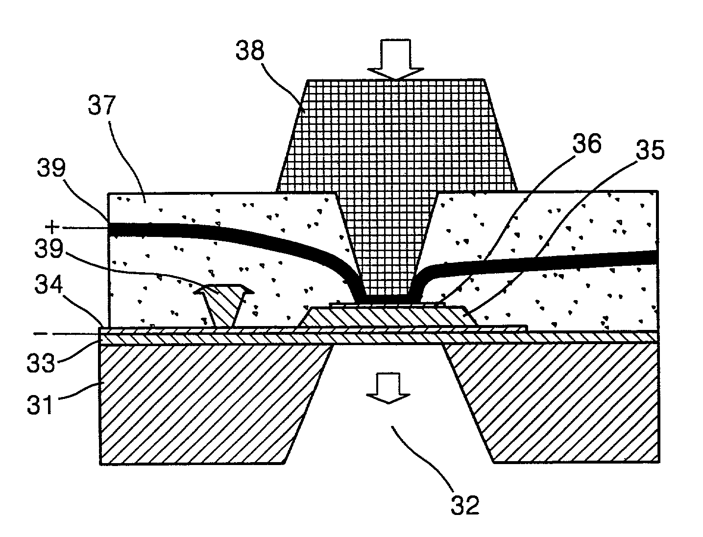
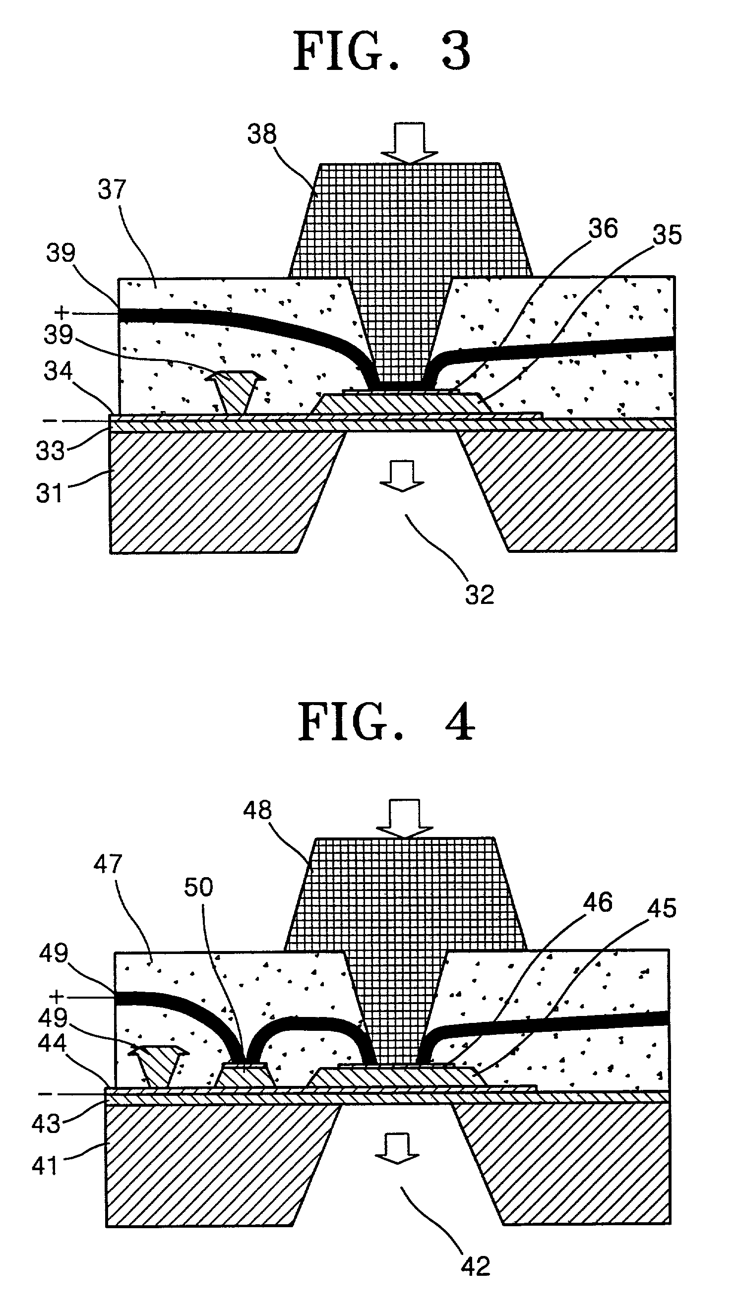
[0029]The structure of a unit piezoelectric device of a fingerprint sensor according to the present invention will be described with reference to FIG. 3.

[0030]A supporting layer 33 is formed on a substrate 31 in which a cavity 32 is formed. A lower electrode 34 is formed on the supporting layer 33. A piezoelectric membrane 35 is formed on a portion of the lower electrode 34 opposite the cavity 32. An upper electrode 36 is formed on the piezoelectric membrane 35. A pressuring portion 38 for applying pressure exerted by contact of a fingerprint of a finger is formed on the upper electrode 36. A non-conductive layer 37 is formed between the pressuring portion 38 and the lower electrode 34. A wiring 39 for transmitting current of the lower and upper electrodes 34 and 36 to the outside is formed in the non-conductive layer 37.

[0031]The supporting layer 33 is not necessary, but maintains elasticity against pressure from the pressuring portion 38 and supports the unit piezoelectric device ...

second embodiment

[0037]A fingerprint sensor according to the present invention will now be described with reference to FIG. 4.

[0038]As shown in FIG. 4, a supporting layer 43 is formed on a substrate 41 in which a cavity 42 is formed. A lower electrode 44 is formed on a predetermined portion of the supporting layer 43.

[0039]A piezoelectric membrane 45 is formed on a portion of the lower electrode 44 opposite the cavity 42. An upper electrode 46 is formed on the piezoelectric membrane 45. A pressuring portion 48 for applying pressure exerted by contact of a fingerprint of a finger is formed on the upper electrode 46. A non-conductive layer 47 is formed between the pressuring portion 48 and the lower electrode 44 and the supporting layer 43. A wiring 49 for transmitting current of the lower and upper electrodes 44 and 46 to the outside is formed in the non-conductive layer 47. Thus, the structure described in the second embodiment is highly similar to the structure described in the first embodiment.

[00...


PUM


Abstract

A fingerprint sensor for sensing a fingerprint by converting pressure applied to a piezoelectric membrane into an electrical signal is provided, wherein the fingerprint sensor having an aggregate of piezoelectric devices includes: a substrate; a lower electrode formed on the substrate; a piezoelectric membrane formed on the lower electrode; an upper electrode formed on the piezoelectric membrane; a pressuring portion formed on the upper electrode for changing a quantity of charge on the piezoelectric membrane due to pressure exerted by contact of a fingerprint; and a non-conductive layer formed on the lower electrode for supporting and exposing the pressuring portion. Thus, a fingerprint sensor having a simple structure is provided, which is able to precisely sense fingerprint information utilizing a piezoelectric phenomenon. The fingerprint sensor may be applied to systems for identifying persons' identities in public institutions and private enterprises, and in individuals' portable systems.

Description

BACKGROUND OF THE INVENTION[0001]1. Field of the Invention[0002]The present invention relates to a fingerprint sensor using a piezoelectric membrane. More particularly, the present invention relates to a fingerprint sensor for sensing a fingerprint by converting pressure applied to a piezoelectric membrane into an electrical signal.[0003]2. Description of the Related Art[0004]Socioeconomic developments have led to off-line direct transactions and cash transactions in the purchase of and payment for goods. To facilitate such transactions, a new form of payment, i.e., using credit cards or on-line e-money, has emerged. As a result, security of one's private information has become a critical issue, and an individual fingerprint sensor is needed to protect an individual's information. In addition, a technique for sensing and deciphering a fingerprint in-situ, where private information is needed, is required.[0005]FIG. 1 shows a perspective view of a conventional fingerprint sensor. Refe...

Claims


Application Information

Patent Timeline
Patent Type & Authority Patents(United States)
IPC IPC(8): G06K9/00G01B7/28A61B5/117G06T1/00H01L41/08
CPCG06K9/0002G06V40/1306G06F18/00
Inventor KIM, CHANG-JUNGPARK, YOUNG-SOOLEE, JUNE-KEY
Owner SAMSUNG ELECTRONICS CO LTD
Why Eureka
Try Eureka