Encapsulated MOS transistor gate structures and methods for making the same

a technology of mos transistor and gate structure, which is applied in the field of mos transistor gate encapsulation and conditioning structure and the like, which can solve the problems of reducing the extent to which siosub>2 /sub>gate dielectric thickness can be reduced, affecting the effect of gate capacitance, and certain high-k dielectric materials being damaged during gate etching

Inactive Publication Date: 2006-03-21
TEXAS INSTR INC
View PDF16 Cites 66 Cited by
  • Summary
  • Abstract
  • Description
  • Claims
  • Application Information

AI Technical Summary

Problems solved by technology

However, limitations on the extent to which SiO2 gate dielectric thicknesses can be reduced have lead to increased usage of so-called high-k dielectric materials having dielectric constants greater than that of SiO2.
However, certain high-k dielectric materials may be damaged during gate etching.
The depleted portion of the gate contact and the gate dielectric operate as series connected capacitors, resulting in a reduced effective gate capacitance, which reduces the drive current capability of the device.
Consequently, poly-silicon depletion causes reduction in device performance and leads to poor unscalable devices, where poly-silicon depletion problems become more significant as device dimensions continue to be scaled.
However, metal gate materials may also be damaged by gate patterning (e.g., etching, wet cleans, etc.) operations, wherein the use of conventional reoxidation encapsulation techniques can actually degrade the damaged metal.
Furthermore, use of traditional oxidation processes in forming an encapsulation layer for patterned metal gate structures may itself cause unwanted oxidation of the metal material, leading to further degradation of device performance.
Furthermore, as discussed above, traditional reoxidation processes may cause formation of low-k dielectrics along the sidewall of high-k gate dielectric layers in the gate stack.

Method used


Image

  • Encapsulated MOS transistor gate structures and methods for making the same
  • Encapsulated MOS transistor gate structures and methods for making the same
  • Encapsulated MOS transistor gate structures and methods for making the same

Examples


Embodiment Construction

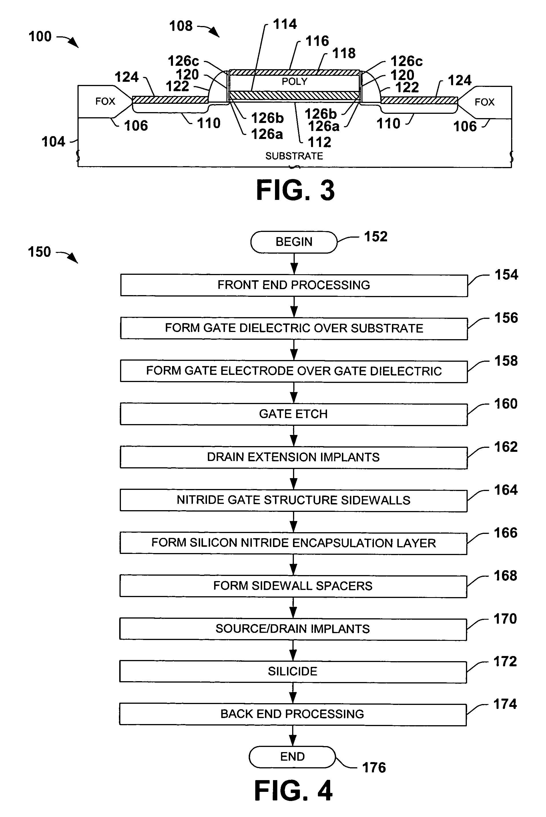
[0019]One or more implementations of the present invention will now be described with reference to the attached drawings, wherein like reference numerals are used to refer to like elements throughout, and wherein the illustrated structures are not necessarily drawn to scale. The invention relates to gate stack fabrication where a gate structure is conditioned through nitridation after gate patterning and encapsulated with a silicon nitride layer.

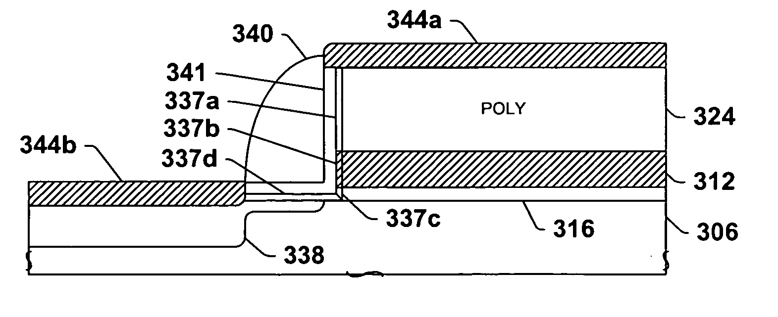
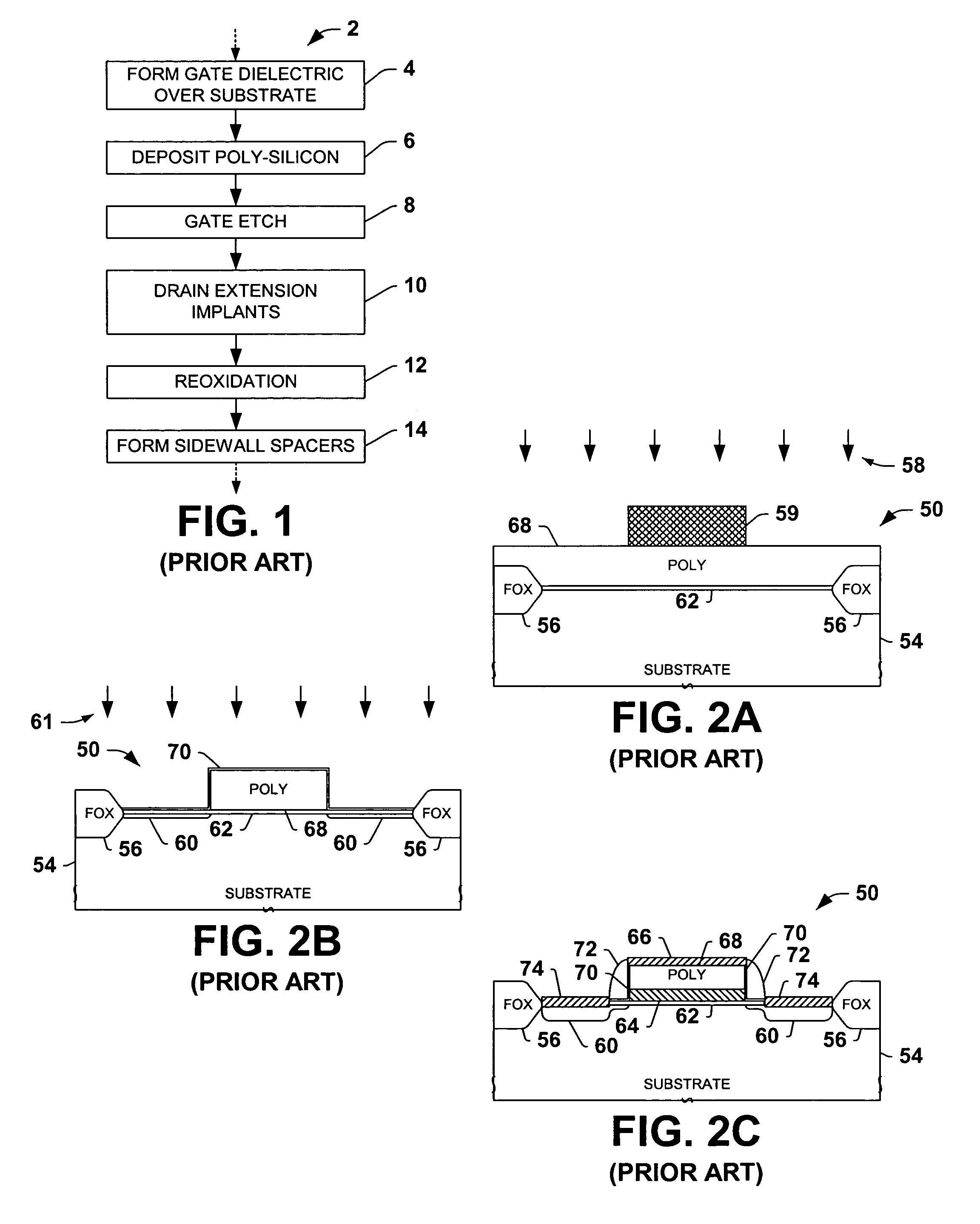
[0020]Referring initially to FIG. 3, a portion of a semiconductor device 100 is illustrated in which an exemplary MOS transistor 108 is formed in accordance with the invention. The device 100 includes a silicon substrate 104 in which field oxide isolation structures 106 are formed, although the invention may be carried out in devices formed using any suitable semiconductor body (e.g., silicon substrates, SOI wafers, epitaxial silicon layers formed above a substrate, etc.) and any suitable isolation structures (e.g., field oxide formed using ...


PUM


Abstract

Transistor gate structures, encapsulation structures, and fabrication techniques are provided, in which sidewalls of patterned gate structures are conditioned by nitriding the sidewalls of the gate structure, and a silicon nitride encapsulation layer is formed to protect the conditioned sidewalls during manufacturing processing. The conditioning and encapsulation avoid oxidation of gate stack layers, particularly metal gate layers, and also facilitate repairing or restoring stoichiometry of metal and other gate layers that may be damaged or altered during gate patterning.

Description

FIELD OF INVENTION[0001]The present invention relates generally to semiconductor devices and more particularly to encapsulation and conditioning structures and techniques for MOS transistor gates.BACKGROUND OF THE INVENTION[0002]Metal-oxide-semiconductor field-effect transistors (MOSFETs) are widely used in the electronics industry for switching, amplification, filtering, and other tasks related to both analog and digital electrical signals. MOS transistors include a gate dielectric overlying a channel region of a semiconductor substrate and a gate electrode situated above the gate dielectric. Source and drain regions are formed in the substrate on either side of the channel. Gate dielectric and gate electrode layers (e.g., silicon dioxide (SiO2) and poly-silicon, respectively) are initially formed over the substrate and the gate electrode is patterned to form a gate structure overlying the channel region of the substrate, after which the source / drain regions are doped with n or p-t...

Claims


Application Information

Patent Timeline
Patent Type & Authority Patents(United States)
IPC IPC(8): H01L29/76H01L29/788H01L21/28H01L21/3205H01L21/336H01L21/4763H01L21/8234H01L21/8242H01L29/49H01L29/78
CPCH01L21/28088H01L29/4966H01L29/6656H01L29/7833H01L29/6659H01L29/665
Inventor COLOMBO, LUIGI
Owner TEXAS INSTR INC
Why Eureka
Try Eureka