Integrated micro electro-mechanical system and manufacturing method thereof

a micro electromechanical and manufacturing method technology, applied in the direction of resilient suspensions, inflated body pressure measurement, chemical vapor deposition coatings, etc., can solve the problem of difficult miniaturization of the entire system, achieve high dimensional accuracy of cavities, improve reliability, and ensure high-quality mechanical characteristics

Active Publication Date: 2006-09-14
HITACHI ASTEMO LTD
View PDF8 Cites 138 Cited by
  • Summary
  • Abstract
  • Description
  • Claims
  • Application Information

AI Technical Summary

Benefits of technology

[0028] In addition, the second primary characteristic of the present invention is that, by forming one integral mechanical structure (including a mass and a movable part considered as a mechanically integral structure) using a plurality of LSI layers or interconnect layers, a movable mass with a sufficient mass required in an acceleration sensor and a gyroscope can be formed through the standard interconnect process of the CMOS process. The movable part of the mechanical structure is preferably formed in a cavity and is fixed to an interlayer dielectric surrounding the cavity by a (elastically) deformable LSI material or metal interconnects. The mechanical structure is designed so that the mechanical characteristics thereof are determined based on the dimensions of the structure itself and do not depend on the shape of the cavity. More specifically, the mechanical structure is provided with (1) a fixed part which is fixed to an interlayer dielectric surrounding a cavity and has an enough size substantially considered to be elastically undeformed, (2) a movable part and (3) an elastically deformable part which connects the fixed part and the movable part. By doing so, the dimensional accuracy of the cavity does not influence the mechanical characteristics of the MEMS. Therefore, the high dimensional accuracy of the cavity is not required in comparison to the case where the mechanical characteristics of the structure depend on the shape of the cavity. Usually, the dimensional accuracy of the structure is defined with the accuracy of the interconnect pattern of a LSI. Since this dimensional accuracy is generally much higher than the process accuracy of the bulk MEMS in the conventional technology, the highly accurate mechanical characteristics can be assured.
[0029] Since the structure is formed by using the interconnect layers, the structure itself has not only the mechanical function as a mass but also the electrical function as an electrode and an interconnect. The actuation and the sensing are performed by the electrostatic force and capacitance between the electrically independent electrode fixed to an interlayer dielectric and a movable part also functioning as an electrode. By using the movable part of the integral structure as a mass, for example, an acceleration sensor and a vibration gyroscope (angle rate sensor) are realized. The mechanical connection between the movable part and the surrounding interlayer dielectric (fixed part and elastically deformable part, for example, beam) and the electrical connection (interconnect, actuator capacitor and detecting capacitor) can be made through separate layers constituting the LSI. By sandwiching the movable part between the multilayer interconnects to restrict the movable range of the movable part, it becomes possible to improve the reliability.

Problems solved by technology

As described above, when the MEMS is used in combination with the signal processing LSI, since each of them is formed on the separate chips, the miniaturization of the entire system is difficult.

Method used


Image

  • Integrated micro electro-mechanical system and manufacturing method thereof
  • Integrated micro electro-mechanical system and manufacturing method thereof
  • Integrated micro electro-mechanical system and manufacturing method thereof

Examples


first embodiment

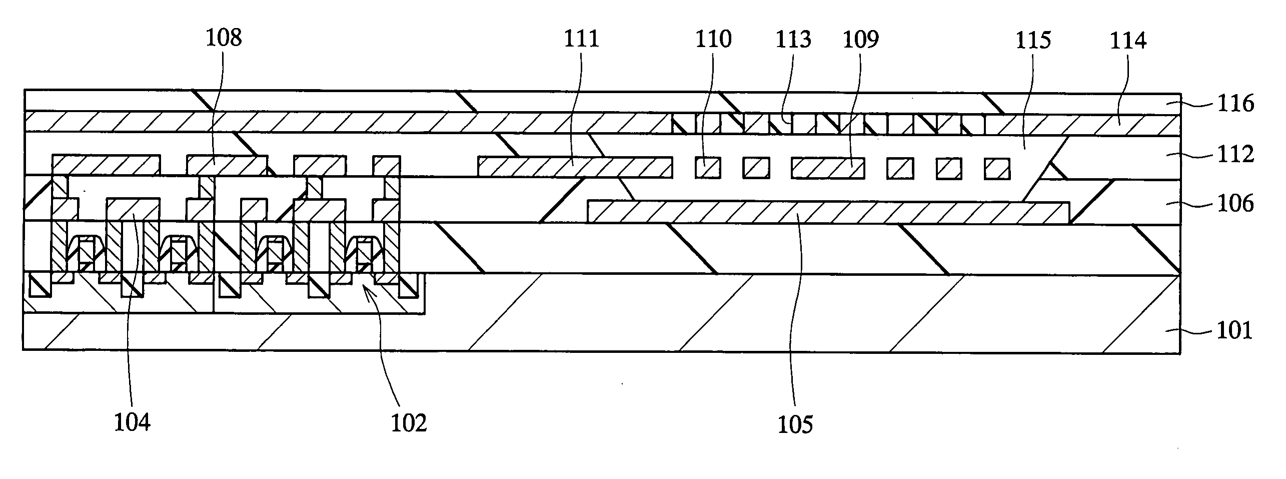
[0101] In the first embodiment, the case where a single axis acceleration (or vibration) sensor is formed as the MEMS will be described.

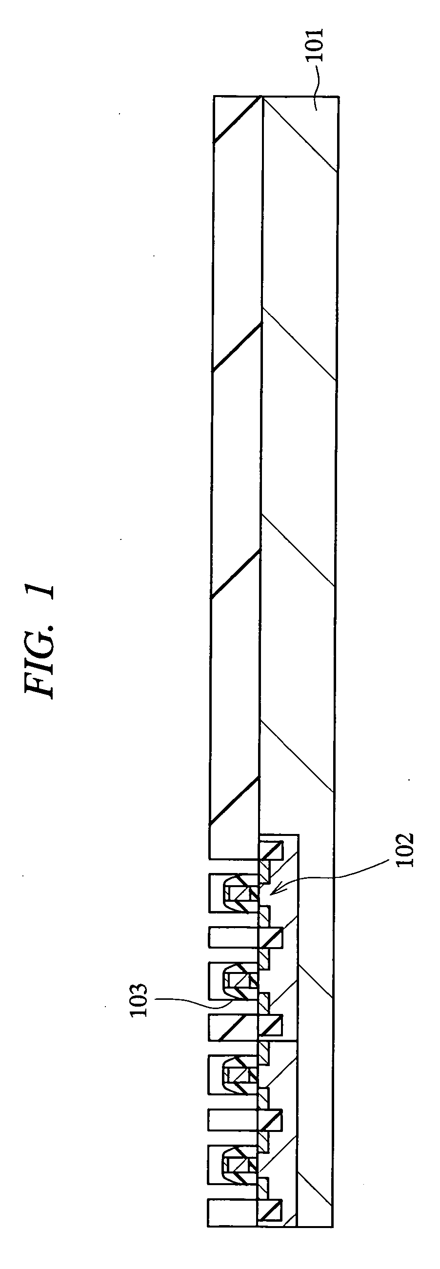
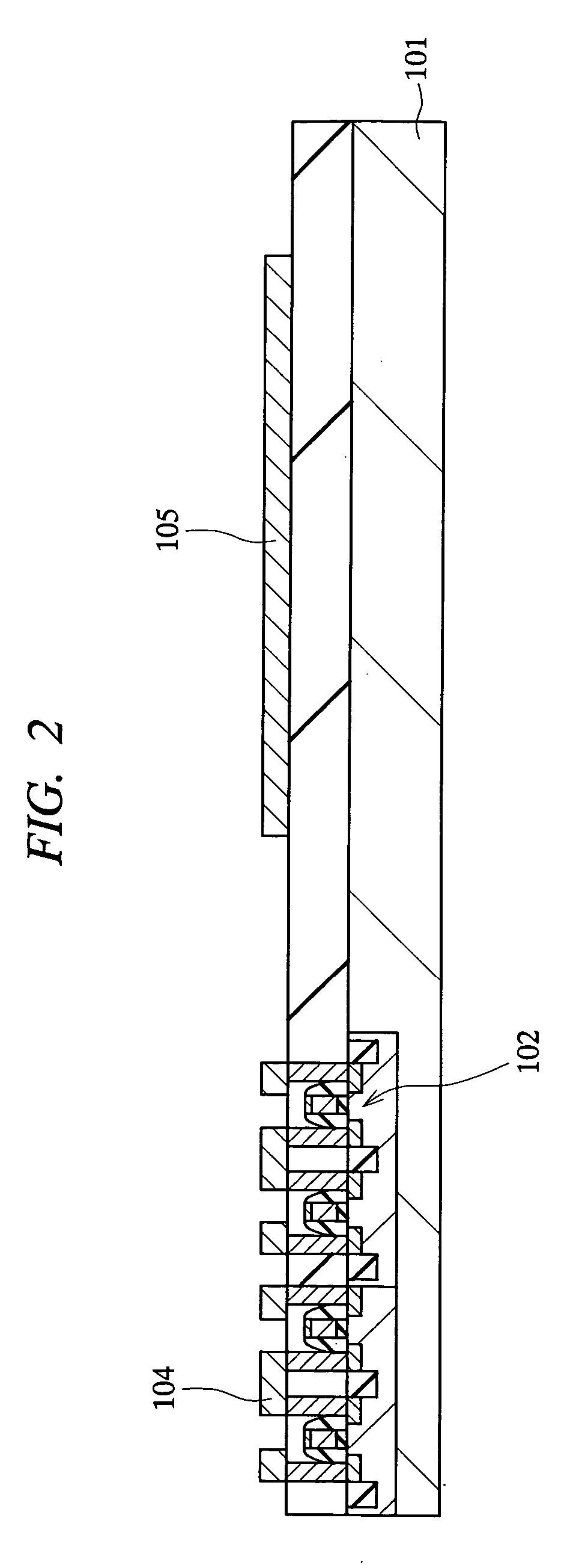
[0102]FIG. 1 to FIG. 8 are schematic diagrams (cross-sectional views) showing the manufacturing process of the integrated MEMS according to the first embodiment. First, in accordance with the normal manufacturing process of a CMOS integrated circuit, transistors 102 for signal processing of the single axis acceleration sensor and contact holes 103 are formed on a silicon substrate (semiconductor substrate) 101 (FIG. 1). Next, by using the manufacturing process of the CMOS integrated circuit, a first layer interconnect (M1 layer) 104 of the signal processing transistors 102 and an etching stopper film 105 used in the etching for forming a cavity (process described later) are formed (FIG. 2).

[0103] Next, through the normal process for manufacturing a CMOS integrated circuit, a multilayer interconnect comprised of a second layer interconnect (M2 laye...

second embodiment

[0120] In this second embodiment, a modification example of the above-described first embodiment will be described. First, in the second embodiment, a 2-axis acceleration sensor which detects the acceleration in two directions within chip (directions orthogonal to each other) will be described. In the acceleration sensor, it is necessary to ensure, a predetermined amount of mass of the movable mass. Therefore, the mechanical structure is formed from a pad layer with a relatively large thickness in the interconnect layers.

[0121]FIG. 12 is a schematic diagram showing the cross-sectional structure of the 2-axis acceleration sensor, and FIG. 13A and FIG. 13B are schematic diagrams showing the configuration of the major layers. In FIG. 12, a movable mass 202, an elastic beam 203 (not shown in FIG. 12) and a fixed capacitor plate (capacitance detecting electrode) 204 of the 2-axis acceleration sensor 201 are formed from the same metal layer as the pad layer 205 of the LSI in which they a...

third embodiment

[0134] In this third embodiment, the MEMS switch mounted together with the LSI will be described. In the third embodiment, the MEMS switch and the integrated circuit are monolithically mounted by using the normal manufacturing technology of a CMOS integrated circuit (interconnect process). Since the MEMS switch is formed on the multilayer interconnect of the integrated circuit, the increase of the chip area can be prevented. The MEMS switches are used to switch the circuit blocks and to switch the input / output RF devices and the antennas in accordance with the RF (Radio Frequency) wireless communication system. By doing so, the connection to low-power-consumption wireless devices and antennas with small loss can be realized.

[0135] First, the function and basic operation of a MEMS switch 300 according to the third embodiment will be described. FIG. 15A to FIG. 15C are plan views schematically showing the configuration and the basic operation of the MEMS switch 300 according to the t...


PUM

PropertyMeasurementUnit
thicknessaaaaaaaaaa
thicknessaaaaaaaaaa
thicknessaaaaaaaaaa

Abstract

In the manufacturing technology of an integrated MEMS in which a semiconductor integrated circuit (CMOS or the like) and a micro machine are monolithically integrated on a semiconductor substrate, a technology capable of manufacturing the integrated MEMS without using a special process different from the normal manufacturing technology of a semiconductor integrated circuit is provided. A MEMS structure is formed together with an integrated circuit by using the CMOS integrated circuit process. For example, when forming an acceleration sensor, a structure composed of a movable mass, an elastic beam and a fixed beam is formed by using the CMOS interconnect technology. Thereafter, an interlayer dielectric and the like are etched by using the CMOS process to form a cavity. Then, fine holes used in the etching are sealed with a dielectric.

Description

CROSS-REFERENCE TO RELATED APPLICATION [0001] The present application claims priority from Japanese Patent Application JP 2005-050541 filed on Feb. 25, 2005 and Japanese Patent Application JP 2005-226233 filed on Aug. 4, 2005, the contents of which are hereby incorporated by reference into this application. TECHNICAL FIELD OF THE INVENTION [0002] The present invention relates to micro electro-mechanical systems (MEMS) and a manufacturing method thereof. More particularly, the present invention relates to a technology effectively applied to an integrated micro electro-mechanical system in which a semiconductor integrated circuit and the MEMS are integrated. BACKGROUND OF THE INVENTION [0003] By using the micro-fabrication technology which has realized the improvement in performance and increase in integration density of the semiconductor integrated circuit, the micro electro-mechanical system (hereinafter, referred to as MEMS) technology for forming a mechanical sensor such as a pres...

Claims


Application Information

Patent Timeline
Patent Type & Authority Applications(United States)
IPC IPC(8): H01L21/00B60C23/04B60C23/20B60G17/00B81B3/00B81B7/02B81C1/00G01C19/56G01C19/5762G01C19/5769G01L9/00G01L17/00G01P15/125G01P15/18H01L21/3205H01L21/768H01L21/8234H01L27/06H01L27/08H01L27/088H01L29/84
CPCB81B2201/0235B81B2201/0264B81C2203/0714B81C2203/0742B81C1/00246B81C2201/014
Inventor FUKUDA, HIROSHIFUJIMORI, TSUKASAYOKOYAMA, NATSUKIHANAOKA, YUKOMATSUMURA, TAKAFUMI
Owner HITACHI ASTEMO LTD
Why Eureka
Try Eureka