Semiconductor storage device and method of manufacturing the same

a technology of semiconductor storage and memory cells, applied in semiconductor devices, diodes, electrical devices, etc., can solve the problems of poor efficiency, inability to easily expand storage capacity, and inability to easily increase memory cell density, so as to prevent the collapse of memory cells during manufacturing processes, improve the effect of efficiency and improve the quality of li

Active Publication Date: 2008-05-08
MICRON TECH INC
View PDF10 Cites 102 Cited by
  • Summary
  • Abstract
  • Description
  • Claims
  • Application Information

AI Technical Summary

Benefits of technology

[0073]As describer above, in the method of manufacture of the semiconductor storage device, a storage element and an N-type semiconductor layer forming a portion of a PN junction diode are formed by filling them in a contact hole, so that collapse of memory cells during manufacturing processes can be prevented.
[0074]Furthermore, the second wire which serve as a word line is formed as a layered member comprising a P-type semiconductor layer and a conductive film, and a PN junction diode is formed from: an N-type semiconductor layer filled in a contact hole provided in an interlayer

Problems solved by technology

Mask ROM, which is one type of OTP memory, records data to memory cells arranged in two dimensions in a plane, and so storage capacity cannot easily be expanded (the memory cell density cannot easily be increased) without enlarging chip sizes.
For this reason, when only a small quantity of chips is to be manufactured with the same content recorded, efficiency is poor, and such memory is uneconomical.
However, although the CVD method is normally on ordinary semiconductor device manufacturing lines to deposit polysilicon films containing phosphorus, in general the CVD method is not used to deposit polysilicon films containing boron or other P-type impurities.
For this reason, when depositing a polysilicon film containing P-type impurities, special dedicated deposition equipment must be prepared, and in general very high costs are incurred to introduce such equipment on semiconductor manufacturing lines, so that such methods cannot easily be applied.
However, when the initially formed undoped polysilicon film has irregularities in the surface, or when the undoped polysilicon film is provided only in the base portions of fine contact holes, impurities cannot be introduced uniformly using ion implantation method, and so the polysilicon film must be deposited in a flat state.
However, as the design rule is reduced and the memory cell shape becomes longer and thinner in the vertical direction compared with the base area, there has been the problem that during cleaning or other wet processes performed during manufacturing, memory cells tend to collapse or are otherwise unstable.
Furthermore, when patterning a plurali

Method used


Image

  • Semiconductor storage device and method of manufacturing the same
  • Semiconductor storage device and method of manufacturing the same
  • Semiconductor storage device and method of manufacturing the same

Examples


first embodiment

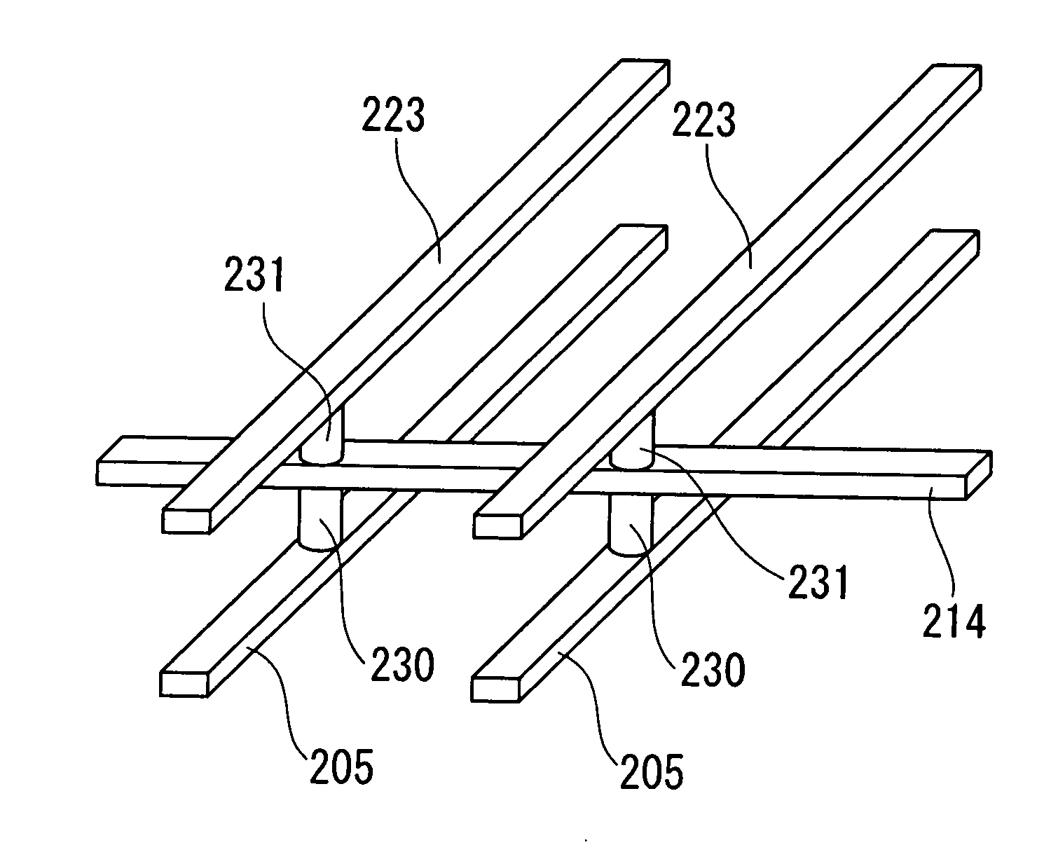
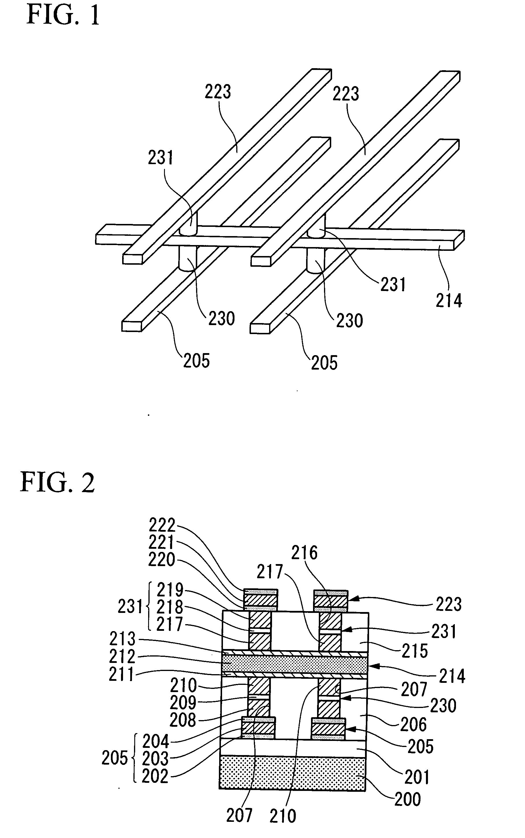
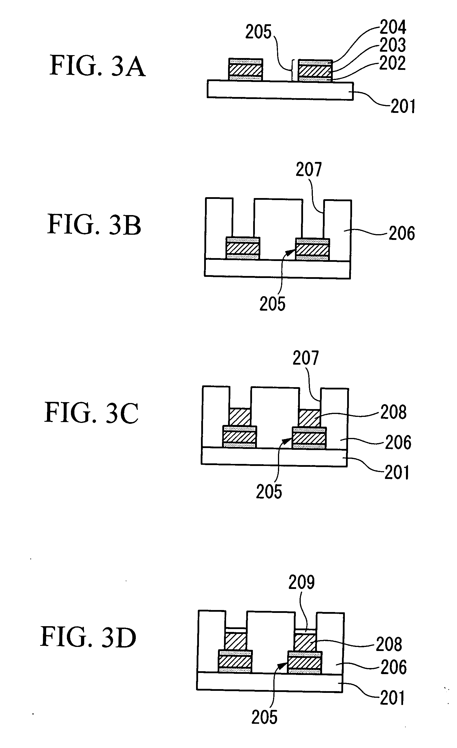
[0092]Hereinbelow, a first embodiment is explained referring to FIG. 1 through FIG. 5B. FIG. 1 is a perspective view showing the configuration of a portion of the semiconductor storage device in accordance with the present embodiment. FIG. 2 is a schematic cross-sectional view showing principal portions of the semiconductor storage device in accordance with the present embodiment. FIG. 3A through FIG. 5B are process diagrams explaining a method of manufacture of the semiconductor storage device shown in FIG. 1 and FIG. 2.

[0093]As shown in FIG. 1, the semiconductor storage device of the present embodiment is mainly configured from first wires 205 extending in one direction, second wires 214 extending in a direction intersecting the first wires 205, and memory cells 230 provided in contact holes positioned at each portion of intersection of first wires 205 and second wires 214, so as to connect the first wires 205 and second wires 214.

[0094]On the opposite side of the second wires 214...

second embodiment

[0136]Next, a second embodiment is explained, referring to FIG. 6 and to FIG. 7A through FIG. 7D. FIG. 6 is a schematic cross-sectional view showing principal portions of the semiconductor storage device in accordance with the present embodiment. FIG. 7A through FIG. 7D are process diagrams used to explain the method of manufacture of the semiconductor storage device shown in FIG. 6. Of the configuration shown in FIG. 6 through FIG. 7D, portions which are the same as in the configurations shown in FIG. 1 through FIG. 5B are assigned the same symbols, and explanations thereof are omitted.

[0137]As shown in FIG. 6, the circuitry necessary for input and output of data to and from memory cells 308 is formed on a semiconductor substrate 200 using MOS type transistors and similar. Furthermore, dielectric film comprising silicon oxide film or similar is formed on the semiconductor substrate 200, and the first wires 205 serving as bit lines are formed on the dielectric film 201; above the fi...

third embodiment

[0152]As a third embodiment, a semiconductor storage device comprising storage elements which utilize the CER phenomenon is explained, referring to FIG. 8. FIG. 8 is a schematic cross-sectional view showing principal portions of the semiconductor storage device in accordance with the present embodiment. Of the configuration shown in FIG. 8, portions which are the same as in the configurations shown in FIG. 1 through FIG. 5B are assigned the same symbols, and explanations thereof are omitted.

[0153]In FIG. 8, a dielectric film 201, formed using a silicon oxide film or similar, is formed on the semiconductor substrate 200. On the dielectric film 201 is formed a laminated film comprising four layers which are a TiN layer 502, a layer 503 of a high-melting point metal such as tungsten, a TiN layer 504, and a Ti (titanium) layer 540; then patterning is performed, to form first wires 505 as bit lines.

[0154]An interlayer dielectric film 506a of silicon oxide or similar is formed so as to co...


PUM


Abstract

A nonvolatile semiconductor storage device is provided in which memory cells comprising PN junction diodes having satisfactory rectifying characteristics are arranged in three dimensions. The semiconductor storage device includes: a first wire which extends in one direction; a second wire which extends in a direction intersecting the first wire; and a memory cell which is positioned at a portion of intersection of the first wire with the second wire between the first wire and the second wire, the memory cell comprising a storage element and a PN junction diode connected thereto, positioned on a side of the second wire used in selecting the memory cell, and a P-type semiconductor forming the PN junction diode forms a portion of the second wire, wherein a plurality of structures, each structure comprising the first wire, the second wire, and the memory cell is provided three-dimensionally.

Description

BACKGROUND OF THE INVENTION[0001]1. Field of the Invention[0002]The present invention relates to a semiconductor storage device and to a method of manufacturing the same, and in particular relates to a nonvolatile semiconductor storage device in which memory cells, comprising combinations of PN junction diodes and storage elements, are positioned in three dimensions, and to a method of manufacturing the same.[0003]Priority is claimed on Japanese Patent Application No. 2006-301478, filed on Nov. 7, 2006, the contents of which are incorporated herein by reference.[0004]2. Description of the Related Art[0005]In recent years, there has been increasing demand for nonvolatile memory, in which there is no loss of stored data even when power is cut off. Nonvolatile memory includes memory types in which recorded data can be modified any number of times, such as NAND flash memory, and memory types such as mask ROM (Read-Only Memory) in which, once data has been recorded, the data cannot be mo...

Claims


Application Information

Patent Timeline
IPC IPC(8): H01L29/04H01L21/20
CPCH01L21/8221H01L27/0688H01L29/8613H01L27/224H01L27/24H01L27/1021H10B61/10H10B63/84H10B63/20H10N70/20H10N70/8836H10N70/231H10N70/8828H10N70/826
Inventor OHARA, SHINJI
Owner MICRON TECH INC
Why Eureka
Try Eureka