Maskless Process for Suspending and Thinning Nanowires

a technology of nanowires and masks, applied in the field of field-effect transistors (fet) devices, can solve the problems of reducing the oxidation rate of nanowires, reducing the charge transport characteristics, and reducing the oxidation ra

Active Publication Date: 2010-08-05
IBM CORP
View PDF21 Cites 140 Cited by
  • Summary
  • Abstract
  • Description
  • Claims
  • Application Information

AI Technical Summary

Benefits of technology

[0005]The present invention provides semiconductor-based electronic devices and techniques for fabrication thereof. In one aspect of the invention, a device is provided comprising a first pad; a second pad and a plurality of nanowires connecting the first pad and the second pad in a ladder-like configuration formed in a silicon-on-insulator (SOI) layer over a buried oxide (BOX) layer, the nanowires having one or more dimensions defined by a re-distribution of silicon from the nanowires to the pads. The device can comprise a field-effect transistor (FET) having a gate surrounding the nanowires wherein portions of the nanowires surrounded by the gate form channels of the FET, the first pad and portions of the nanowires extending out from the gate adjacent to the first pad form a source region of the FET and the second pad and portions of the nanowires extending out from the gate adjacent to the second pad form a drain region of the FET.

Problems solved by technology

The scale of these variations can be a significant fraction of the nanowire size, and can thus lead to perturbations in the channel potential and scattering that degrade the charge transport characteristics.
However, the oxidation rate of nanowires can be substantially slower than planar silicon (Si), with the oxidation rate dropping with smaller diameter nanowires.
As such, the oxidation time required for thinning of nanowires can undesirably result in the complete oxidation of the planar Si in the source and drain regions.
Stress in the mask can lead to an uneven oxidation at the mask's edge, which leads to non-uniform thinning of the nanowires.

Method used


Image

  • Maskless Process for Suspending and Thinning Nanowires
  • Maskless Process for Suspending and Thinning Nanowires
  • Maskless Process for Suspending and Thinning Nanowires

Examples


Embodiment Construction

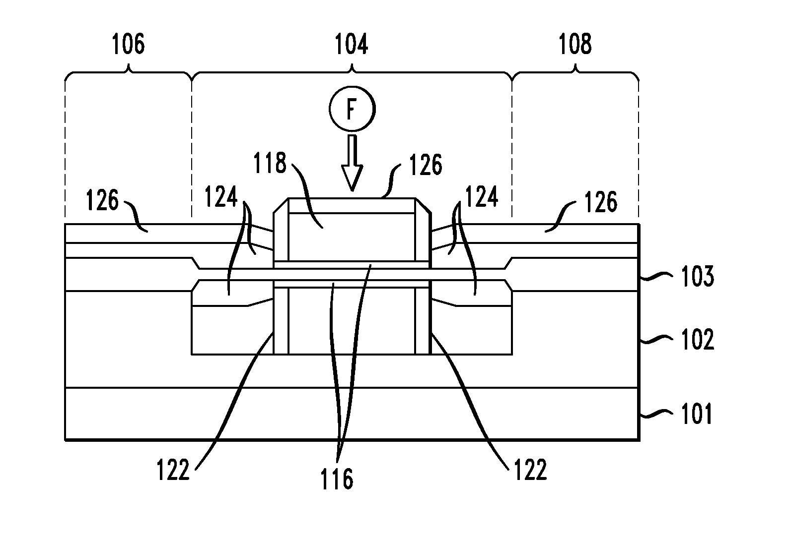
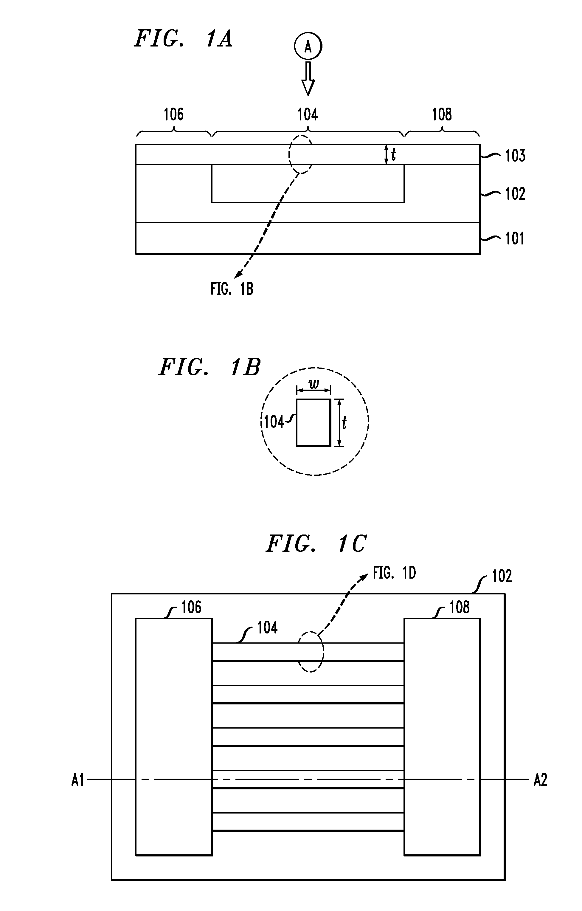
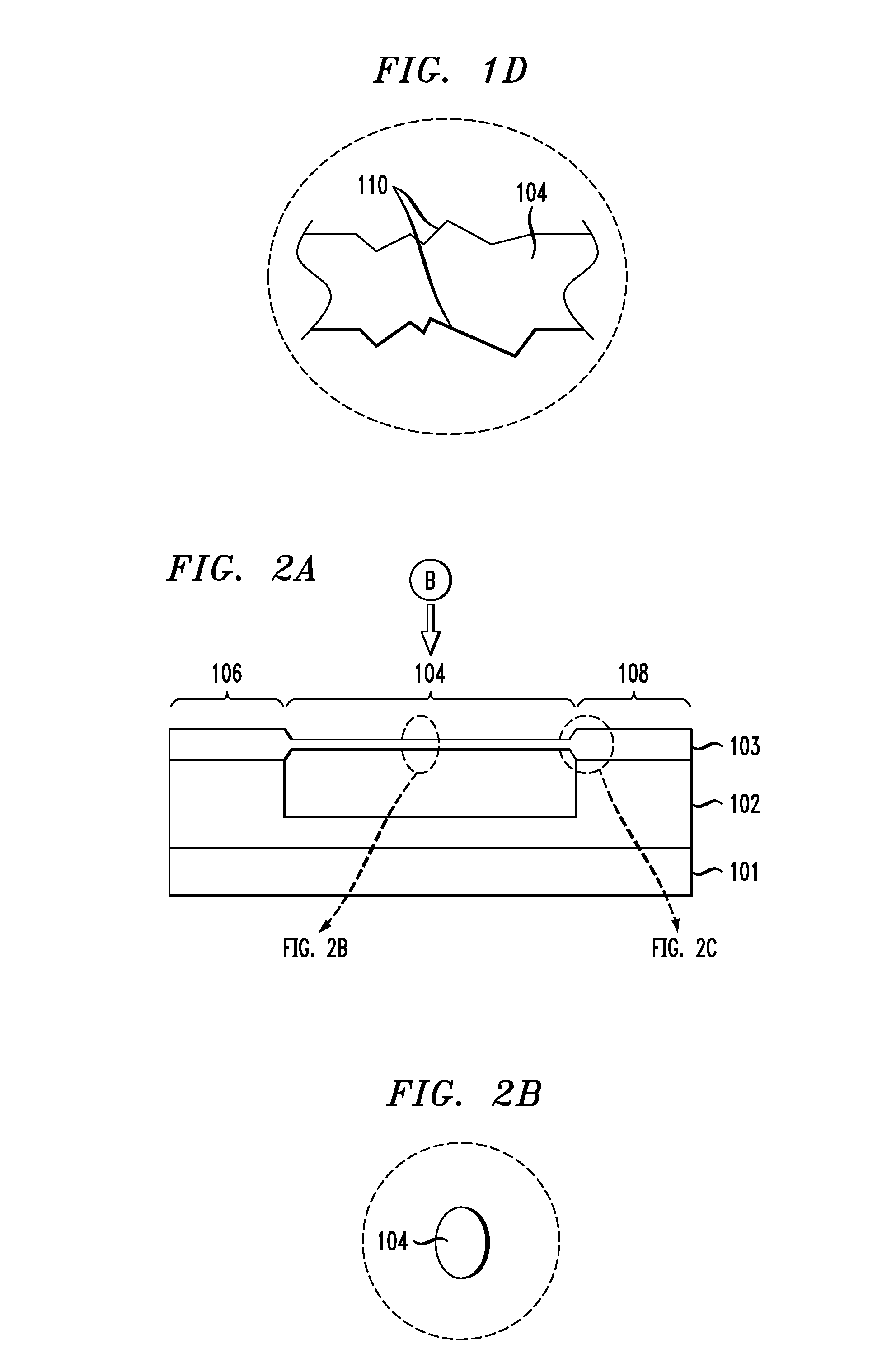
[0023]The present techniques provide a gate-all-around (GAA) nanowire field-effect transistor (FET) as well as methods for fabricating the same. In this discussion, reference will be made to various drawings that illustrate embodiments of the present teachings. Since the drawings of the embodiments of the present teachings are provided for illustrative purposes, the structures contained therein are not drawn to scale.

[0024]The present methods are described using silicon (Si) nanowires and Si processing. However, the present techniques can also be practiced with other semiconductor materials such as, for example, germanium (Ge) or III-V semiconductors. When non-Si-containing semiconductors are used, the processing steps of the present teachings are basically the same except that growth temperature and dopant species applied are adapted to the specific semiconductor used. Use of Si-containing semiconductor materials such as Si, silicon germanium (SiGe), Si / SiGe, silicon carbide (SiC) ...


PUM


Abstract

Semiconductor-based electronic devices and techniques for fabrication thereof are provided. In one aspect, a device is provided comprising a first pad; a second pad and a plurality of nanowires connecting the first pad and the second pad in a ladder-like configuration formed in a silicon-on-insulator (SOI) layer over a buried oxide (BOX) layer, the nanowires having one or more dimensions defined by a re-distribution of silicon from the nanowires to the pads. The device can comprise a field-effect transistor (FET) having a gate surrounding the nanowires wherein portions of the nanowires surrounded by the gate form channels of the FET, the first pad and portions of the nanowires extending out from the gate adjacent to the first pad form a source region of the FET and the second pad and portions of the nanowires extending out from the gate adjacent to the second pad form a drain region of the FET.

Description

FIELD OF THE INVENTION[0001]The present invention relates to semiconductor-based electronic devices, and more particularly, to field-effect transistor (FET) devices having nanowire channels and techniques for fabrication thereof.BACKGROUND OF THE INVENTION[0002]Gate length scaling of gate-all-around (GAA) field-effect transistors (FETs) with nanowire channels can be achieved provided that the nanowire channel diameter can be reduced. For example, scaling of a GAA metal-oxide semiconductor field-effect transistor (MOSFET) to sub-20 nanometer (nm) gate length requires nanowire channels with a diameter of less than 10 nm. See, for example, Oh et al., “Analytic Description of Short-Channel Effects in Fully-Depleted Double-Gate and Cylindrical, Surrounding-Gate MOSFETs,” Electron Dev. Lett., vol 21, no. 9, pgs. 445-47 (2000). Fabricating nanowires at this scale with current lithographic capabilities introduces large variations, both in nanowire size and in line edge roughness (LER). The ...

Claims


Application Information

Patent Timeline
Patent Type & Authority Applications(United States)
IPC IPC(8): H01L29/78H01L21/4763H01L21/84
CPCB82Y10/00H01L29/78696H01L21/02532H01L21/02603H01L21/0262H01L21/02639H01L21/02667H01L29/0665H01L29/0673H01L29/66439H01L29/775Y10S977/762B82Y40/00H01L29/42392H01L21/02488
Inventor BANGSARUNTIP, SARUNYACOHEN, GUYSLEIGHT, JEFFREY W.
Owner IBM CORP
Why Eureka
Try Eureka