Exposure device, exposure method and method of manufacturing semiconductor device

a semiconductor device and exposure device technology, applied in the direction of photomechanical equipment, instruments, printers, etc., can solve the problems of large leak current, high operation speed and driving performance, and variable characteristics of tfts

Inactive Publication Date: 2006-04-04
SEMICON ENERGY LAB CO LTD
View PDF48 Cites 127 Cited by
  • Summary
  • Abstract
  • Description
  • Claims
  • Application Information

AI Technical Summary

Problems solved by technology

However, the TFT having an active layer of crystalline semiconductor film involves a problem in that the TFT is, on one hand high in operation speed and driving performance, but on the other hand large in leak current as compared to a TFT having an active layer of an amorphous semiconductor film.
The problem accompanying this method is that characteristics of TFTs vary because the positioning of the photo mask is uneven in a certain range.
However, in patterning by exposure from the back side in prior art, light goes around and reaches over, resulting in a slightly narrower pattern than the width of the wiring.
The problem this method gives rise to is that forming the resist pattern as desired is difficult because the resist pattern can be formed only one having almost the same size as the gate wiring used for a mask.
For that reason, particularly when a minute wiring is used as a mask, the method is not suitable, for a fear that the entire resist over the wiring may be exposed.
In addition, to cause the light to round and reach the point about 1 μm far from the end, considerable exposure time and exposure light quantity are required.

Method used


Image

  • Exposure device, exposure method and method of manufacturing semiconductor device
  • Exposure device, exposure method and method of manufacturing semiconductor device
  • Exposure device, exposure method and method of manufacturing semiconductor device

Examples


embodiment mode 1

(Embodiment Mode 1)

[0062]Hereinbelow, a description will be made on an example of an embodiment mode of the present invention with reference to FIG. 6.

[0063]As shown in FIG. 6, an exposure device of the present invention comprises: a stage for placing a light transmissive substrate on which a photosensitive thin film is formed; a light source for exposing the photosensitive thin film to light; and a reflecting means disposed on the front side of the light transmissive substrate. A substrate on which a metal thin film with reflectivity is formed (reflecting plate), a mirror or a light scattering plate is used as a reflecting means 602, and arranged in parallel to the substrate surface. A distance X between the reflecting means and the photosensitive thin film surface is adjusted within a range of from 0.1 μm to 1000 μm, thereby controlling a distance Y for light to round.

[0064]In an exposure method of the present invention, light 601 from the light source which has penetrated the pho...

embodiment mode 2

(Embodiment Mode 2)

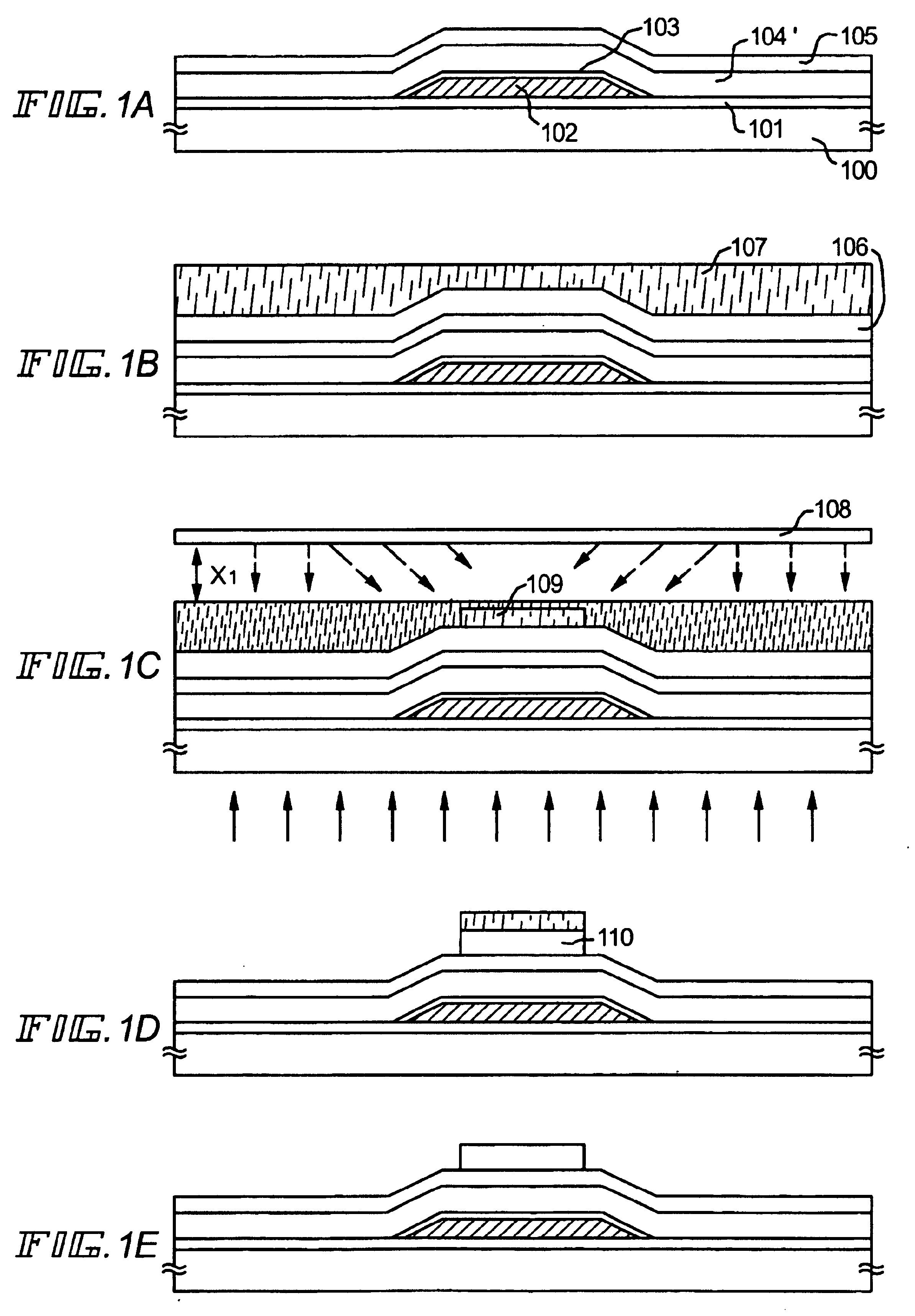
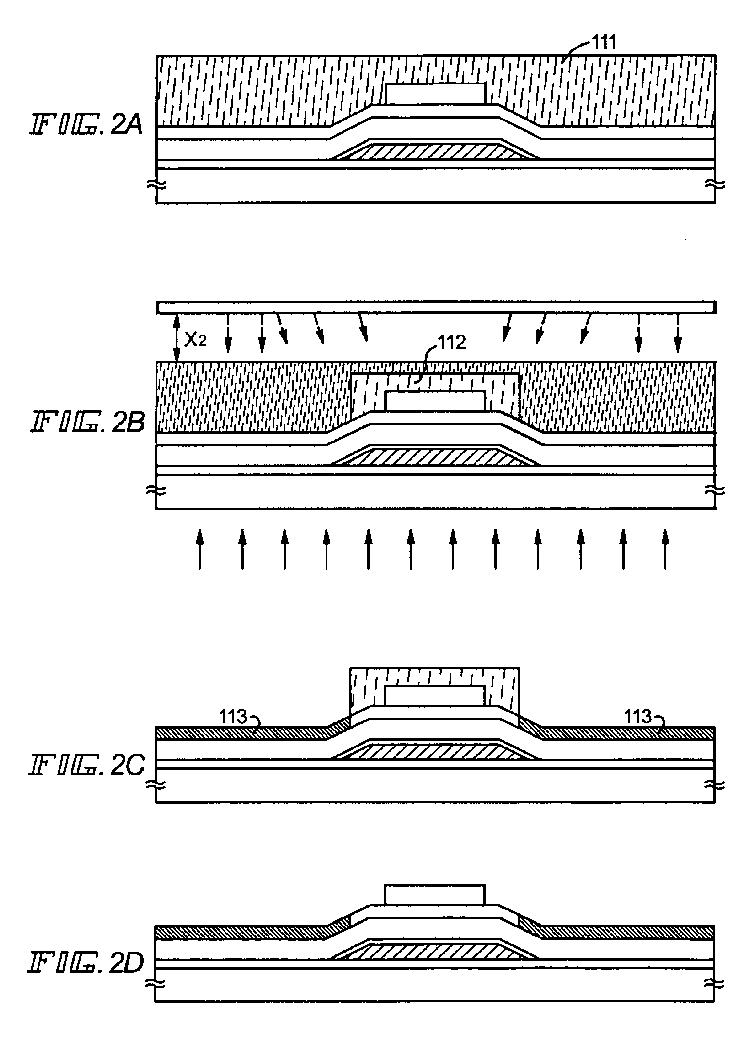
[0071]A detailed description will be made below on an example of an embodiment mode according to the present invention, with reference to FIGS. 1A to 1E. For the purpose of simplification, a manufacturing method using an n-channel TFT will be explained.

[0072]A substrate is first prepared. Usable substrate as a substrate 100 includes an insulating substrate such as a glass substrate, a quartz substrate or a crystalline glass substrate, and a substrate having light transmittance such as a plastic substrate (polyethylene terephtalate substrate).

[0073]Next, a base insulating film (hereinafter, referred to as base film) 101 is formed on the substrate and thermally processed. This base film 101 may be a silicon oxide film, a silicon nitride film or a silicon nitride oxide film (SiOxNy), or may be a laminate film of those. The film thickness of the base film ranges from 100 nm to 500 nm. As formation method of the base film, thermal CVD, plasma CVD, sputtering, evaporati...

embodiment 1

[Embodiment 1]

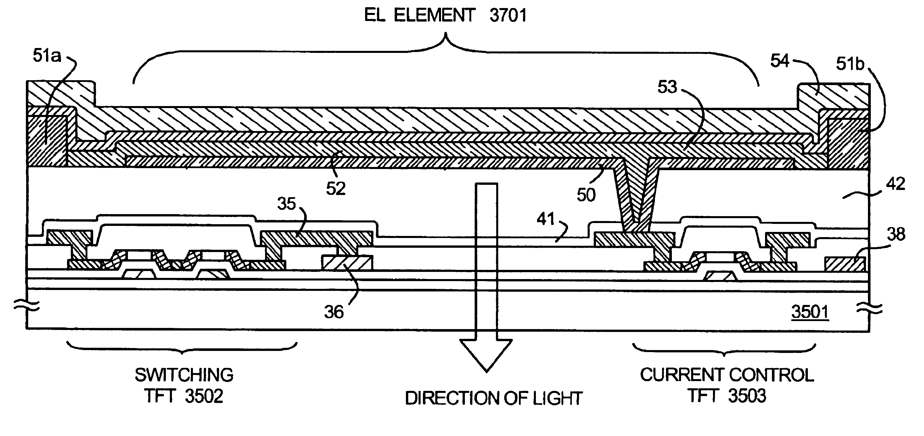
[0101]This embodiment takes an example of fabricating a CMOS circuit, which constitutes a part of a peripheral driver circuit, and a pixel TFT, which constitutes a part of a pixel portion, over the same substrate, using the present invention. Explanation is briefly given below with reference to FIGS. 1A to 5B, which are simplified sectional views showing a semiconductor device of the present invention and a method of manufacturing the same. For the purpose of simplification, an n-channel TFT is used for the detailed description on the manufacturing method in this embodiment.

[0102]First, a light transmissive substrate 100 is prepared. A glass substrate (Corning 1737; with a strain point of 667° C.) is used as the substrate 100 in this embodiment. A base insulating film (hereinafter in this specification, referred to as base film) is formed on the substrate 100 and then thermally processed. The thermal processing here is performed at a temperature below the strain point ...


PUM

PropertyMeasurementUnit
sizeaaaaaaaaaa
distanceaaaaaaaaaa
transmittanceaaaaaaaaaa

Abstract

The present invention provides a highly controllable device for exposure from the back side and an exposure method, and also provides a method of manufacturing a semiconductor device using the same. The present invention involves exposure with the use of the back side exposure device of which a reflecting means is disposed on the front side of a substrate, apart from a photosensitive thin film surface by a distance X(X=0.1 μm to 1000 μm), and formation of a photosensitive thin film pattern in a self alignment manner, with good controllability, at a position a distance Y away from the end of a pattern. The invention fabricates a TFT using that method.

Description

BACKGROUND OF THE INVENTION[0001]1. Field of the Invention[0002]The present invention relates to an exposure device and an exposure method. The invention also relates to a semiconductor device having a circuit that is composed of a thin film transistor (hereinafter referred to as TFT) made by using the exposure method, and to a method of manufacturing the same. The semiconductor device of the present invention includes not only elements such as thin film transistors (TFTs) and MOS transistors but also electrooptical devices, such as display devices and image sensors, having semiconductor circuits composed of those insulating gate type transistors. The semiconductor device of the invention relates to, for example, electrooptical devices typical example of which is a liquid crystal display panel or an electroluminescence (EL) display device and to electronic equipments provided with as their parts such electrooptical devices.[0003]Incidentally, the semiconductor device in this specifi...

Claims


Application Information

Patent Timeline
Patent Type & Authority Patents(United States)
IPC IPC(8): H01L21/84H01L21/00G03B27/00G03F7/00G09G3/32H01L21/265H01L21/336H01L21/77H01L27/12
CPCG03B27/00H01L21/0273G03F7/702H01L27/1214H01L29/66765G03B27/16H01L27/12G09G3/3208H01L27/1288
Inventor ADACHI, HIROKI
Owner SEMICON ENERGY LAB CO LTD
Why Eureka
Try Eureka