Interface device

Inactive Publication Date: 2006-04-18
STMICROELECTRONICS LTD
View PDF12 Cites 32 Cited by
  • Summary
  • Abstract
  • Description
  • Claims
  • Application Information

AI Technical Summary

Benefits of technology

[0017]According to a still further aspect of the invention there is provided a method of debugging a target integrated circuit chip having a digital processor and an on-chip emulator wherein said on-chip emulator is operable to control said digital processor and to collect operation data from said digital processor for communicating to a host, said chip comprising a target on-chip universal serial bus interface connected to said on-chip emulator, the method comprising, providing a communication device comprising an Ethernet port, a universal serial bus port and a further integrated circuit chip having on-chip processing circuitry, on-chip memory circuitry, an on-chip Ethernet interface and an on-chip universal serial bus interface, connecting said Ethernet port to said host; connecting said communication device to said target on-chip universal serial bus interface via a universal serial bus; communicating data between said on-chip emulator and said on-chip processing circuitry; processing said data in said on-chip processing circuitry to provide output data; supplying said output data to said on-chip emulator circuitry.

Problems solved by technology

There is however a problem in that the use of a specialized link dictates a physical link dedicated to the system, and also requires the host computer to be running programs dedicated to the production of signals for the on-chip emulation device of concern.

Method used


Image

  • Interface device
  • Interface device
  • Interface device

Examples


Embodiment Construction

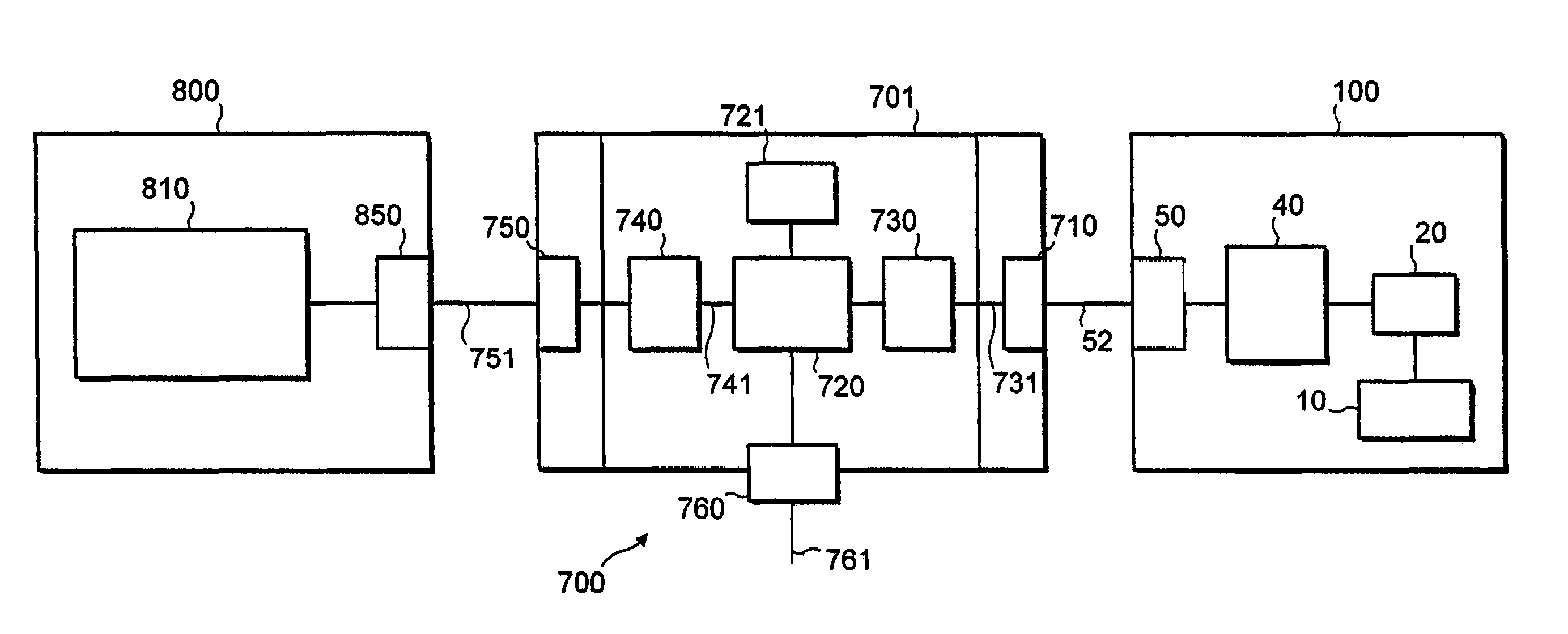
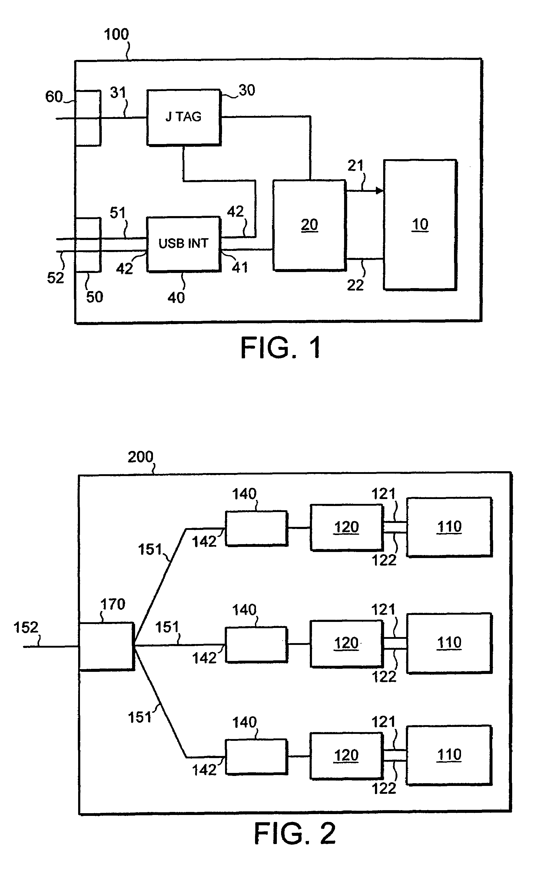
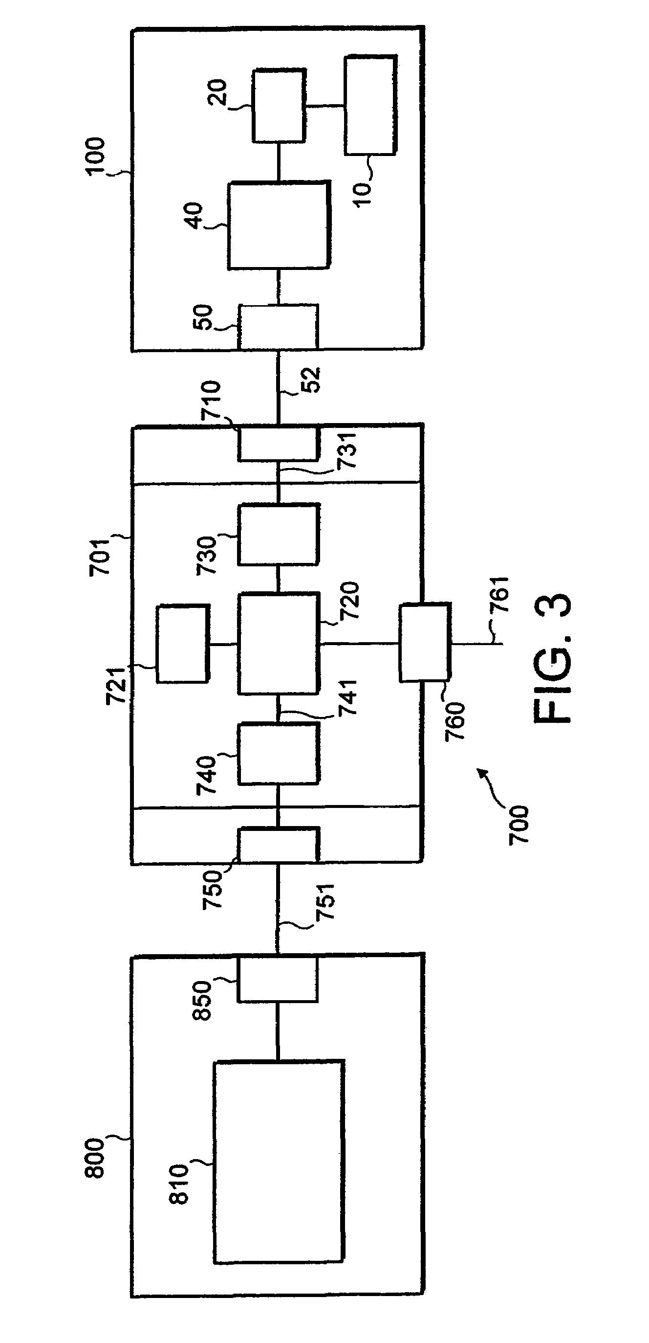
[0024]Referring first to FIG. 1, an embedded system includes an integrated circuit chip 100 which comprises a processor 10 on said chip. As used herein, the term ‘processor’ includes microprocessors and digital signal processors. The processor is connected to other component circuitry of said embedded system in a manner known to those skilled in the art.

[0025]At least during debugging of said embedded system, it is advantageous to be able to collect information about the operation of the processor and also to supply control and command information to said processor, both in response to conditions on the processor itself, and also in response to information conveyed from a host computer.

[0026]For collecting information about operation of the processor and for controlling the processor the chip 100 includes an “on-chip emulator” which comprises storage and processing circuitry for that purpose. Such an on-chip emulator 20 is shown schematically on FIG. 1 as having a control path 21 co...


PUM


Abstract

A communication device for a target integrated circuit chip having a digital processor, an on-chip emulator for controlling the digital processor and for collecting operation data from the digital processor for communicating to off-chip circuitry, and a target on-chip universal serial bus interface connected to the on-chip emulator, the communication device including an Ethernet port, an universal serial bus port and a further integrated circuit chip having on-chip universal serial bus interface, the on-chip Ethernet interface being connected to the Ethernet port, the interfaces being connected to the processing circuitry for translating between Ethernet protocol data on an Ethernet bus connected to the Ethernet port and universal serial bus data for the target on-chip universal serial bus interface.

Description

FIELD OF THE INVENTION[0001]The present invention relates to a communication device suitable for debugging a digital processor on a single integrated circuit chip, the chip comprising an on-chip emulation device.BACKGROUND TO THE INVENTION[0002]Known techniques for debugging embedded digital processors include the use of on-chip emulation devices whose function is to monitor and control the operation of the digital processor. Such on-chip emulation devices typically have storage capability, and the ability to initiate command and control sequences for the digital processor in response to externally applied signals from a host computer or to detected states of the digital processor.[0003]Communication between the on-chip emulation device (oce) and the host computer is carried out via a link, which is typically a link designed for the particular situation. As a result, signals over the link may be tailored to the particular on-chip emulation device in the interests of efficient debugg...

Claims


Application Information

Patent Timeline
Patent Type & Authority Patents(United States)
IPC IPC(8): G06F9/455G06F11/36
CPCG06F11/3656G06F11/3636
Inventor DEBLING, ANTHONY
Owner STMICROELECTRONICS LTD
Why Eureka
Try Eureka