Optical scanning device and image forming apparatus using the same
a scanning device and scanning device technology, applied in the field of optical scanning devices and image forming apparatuses, can solve the problems of color displacement in the obtained image, image performance degradation, and difficulty in simultaneously correcting the scan line bending for plural light beams, and achieve the effect of increasing the number of constituent elements
- Summary
- Abstract
- Description
- Claims
- Application Information
AI Technical Summary
Benefits of technology
Problems solved by technology
Method used
Image
Examples
embodiment 1
[Embodiment 1]
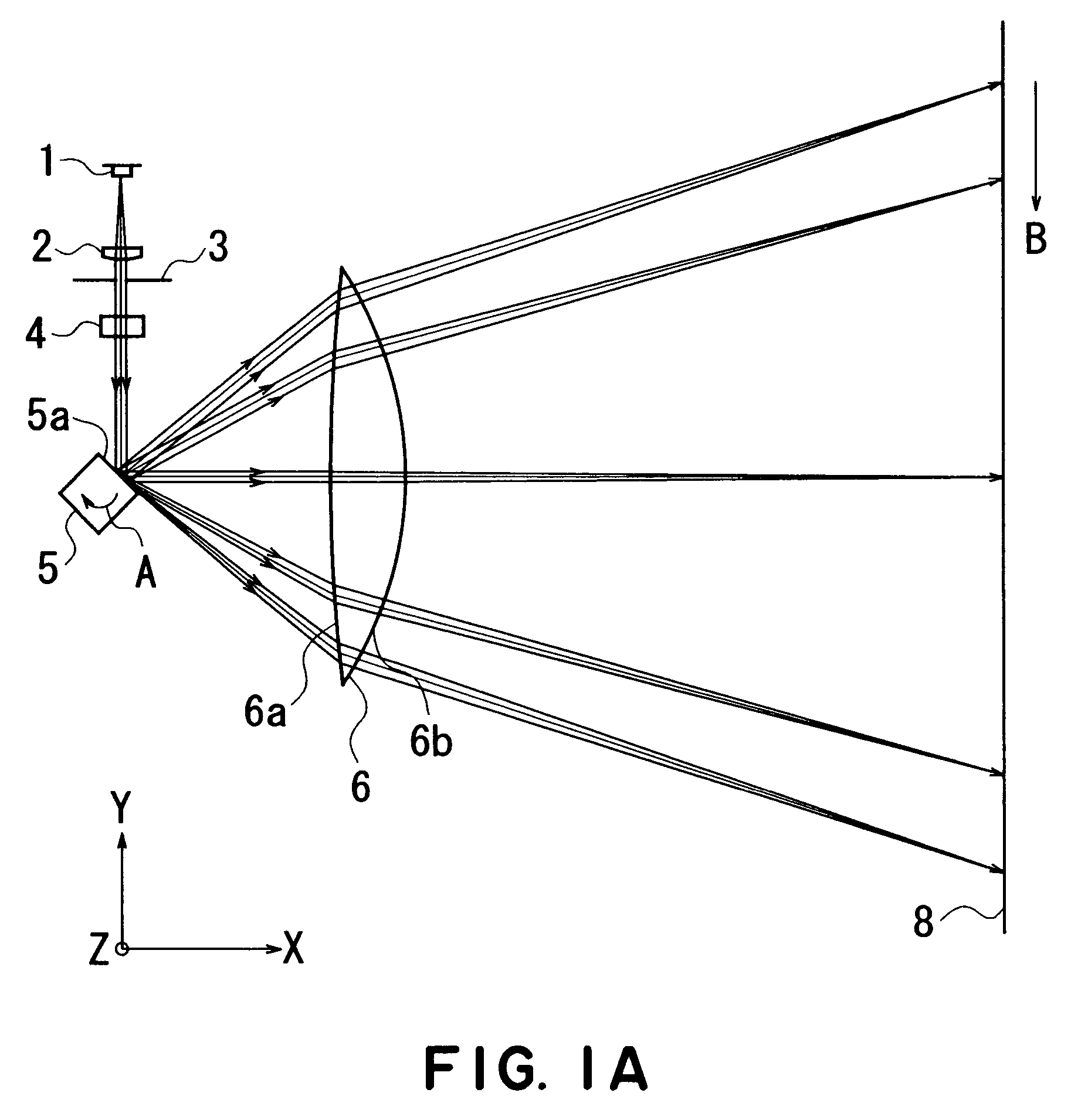
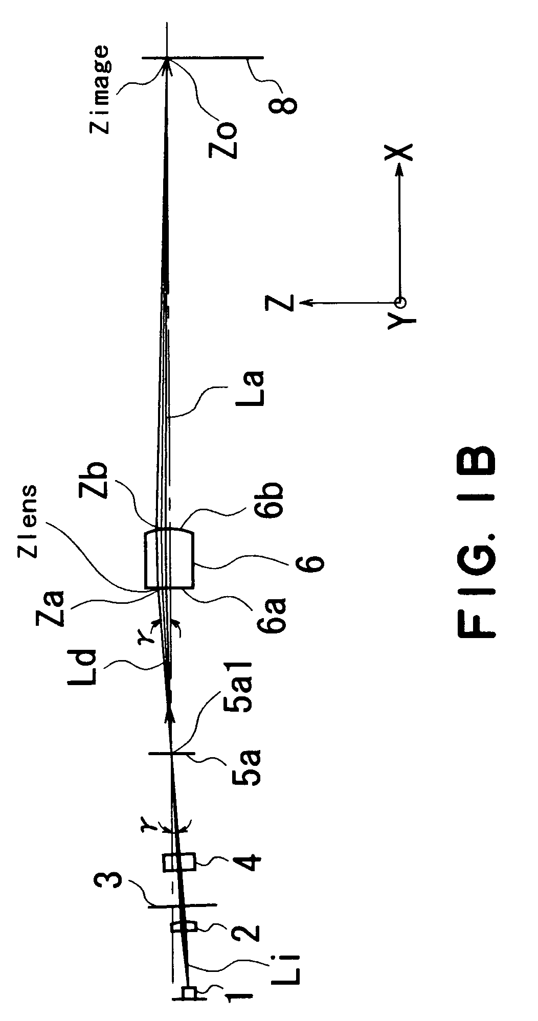
[0099]FIG. 1A is a sectional view (main-scan sectional view) of a main portion of an optical scanning device in a main scan direction, according to a first embodiment of the present invention. FIG. 1B is a sectional view (sub-scan sectional view) of the main portion of the optical scanning device in the first embodiment.
[0100]Here, the term “main scan direction” refers to a direction perpendicular to a rotational axis of deflecting means and an optical axis of a scanning optical element (i.e., a direction in which a light beam is reflectively deflected (deflectively scanned) by the deflecting means). The term “sub-scan” refers to a direction parallel to the rotational axis of the deflecting means. The term “main-scan sectional plane” refers to a plane which contains the optical axis of the scanning optical system. The term “sub-scan sectional plane” refers to a sectional plane perpendicular to the main-scan sectional plane.
[0101]In FIGS. 1A and 1B, denoted at 1 is a se...
embodiment 2
[Embodiment 2]
[0154]FIGS. 12A and 12B are schematic views, respectively, along a sub-scan sectional plane of an optical scanning device according to a second embodiment of the present invention.
[0155]The second embodiment differs from the first embodiment in that the sagittal aspherical amount of the exit surface 6b of the scanning optical element 6 is changed.
[0156]Table 3 below shows the shapes of the entrance surface 6a and exit surface 6b of the scanning optical element 6 in the second embodiment.
[0157]
TABLE 3STRUCTURE OF OPTICAL SCANNING DEVICEf-θ COEFF.,SCAN WIDTH, ANGLE OF VIEWf-θ LENS 6 MERIDIONAL SHAPEf-θ LENS 6 SAGITTAL SHAPEf-θ COEFF.k (mm / 150ENTRANCEEXITENTRANCEEXITrad)SURFACE 6aSURFACE 6bSURFACE 6aSURFACE 6bSCAN WIDTHW214LIGHTLIGHTLIGHTLIGHT(mm)SOURCESOURCESOURCESOURCESIDESIDESIDESIDEMAXIMUM ANGLEθ (deg)40.87R 4.27400E+00−9.47135E+01Rsinfinite−2.39398E+01OF VIEWWAVELENGTH, REFRACTIVITYK 3.71366E+00 0.00000E+00D20.00000E+00 6.55434E−05USED WAVELENGTHλ (nm)780B4−1.85091E−...
embodiment 3
[Embodiment 3]
[0201]FIG. 17A is a main-scan sectional view of an optical scanning device according to a third embodiment of the present invention, and FIG. 17B is a sub-scan sectional view of the same.
[0202]The third embodiment includes two optical scanning devices according to the first or second embodiment, but single deflecting means is shared by them. More specifically, the third embodiment concerns an optical scanning device for a color image forming apparatus wherein two light beams are inputted to each scanning optical system 6 and, thus, four light beams are projected simultaneously upon single deflecting means 5, such that our light beams are deflected by the single deflecting means 5 to thereby optically scan photosensitive drums 8a–8d corresponding to the four light beams, respectively.
[0203]In FIGS. 17A and 17B, denoted at 1 is light source means (multi-beam laser) which comprises four semiconductor lasers 1a, 1b, 1c and 1d each being adapted to emit a single light beam....
PUM
 Abstract
Description
Claims
Application Information


