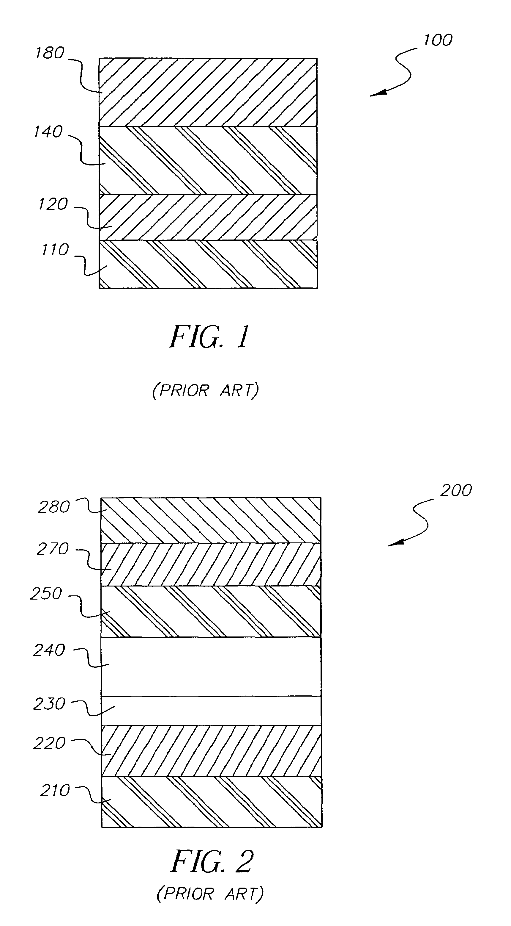
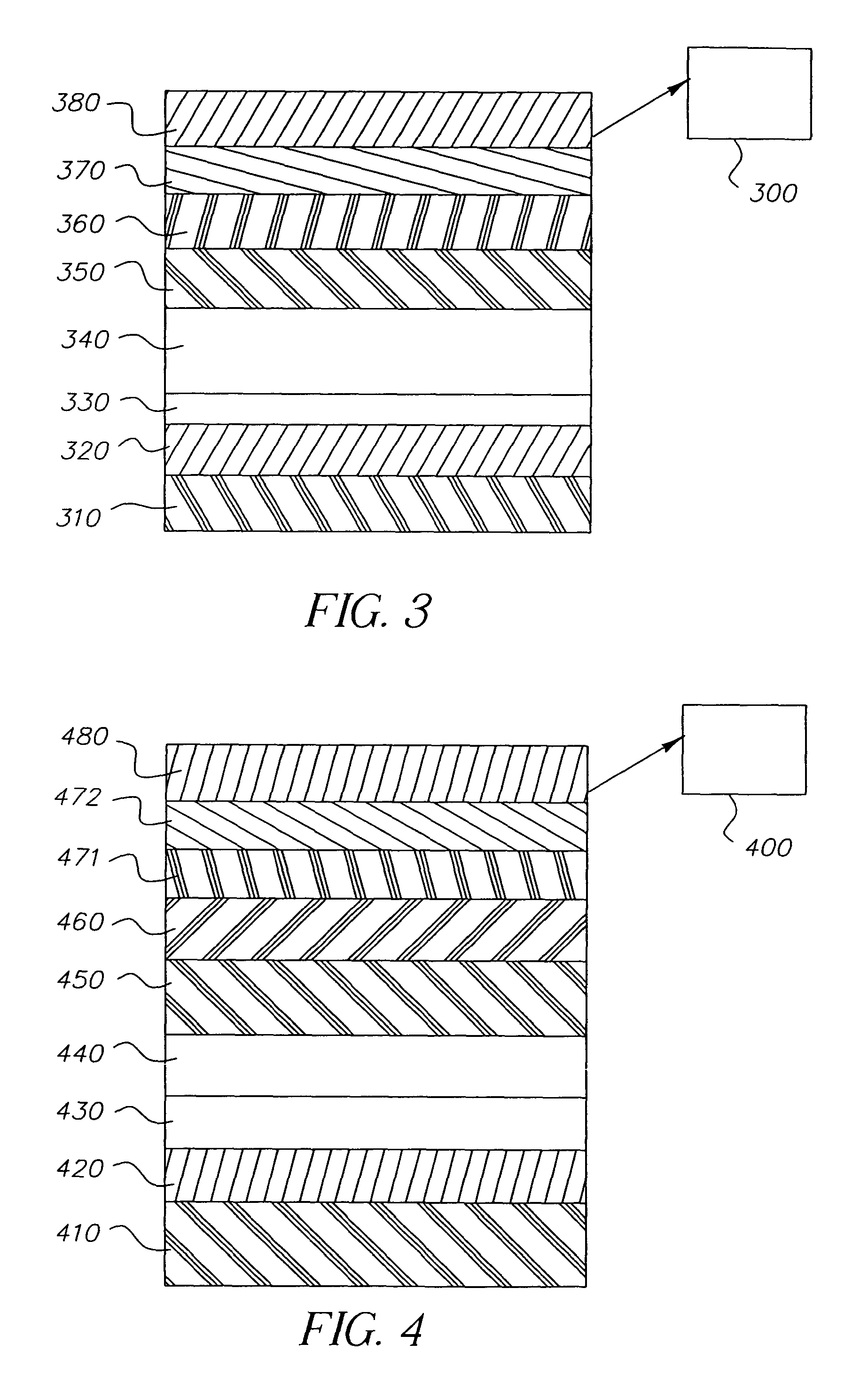
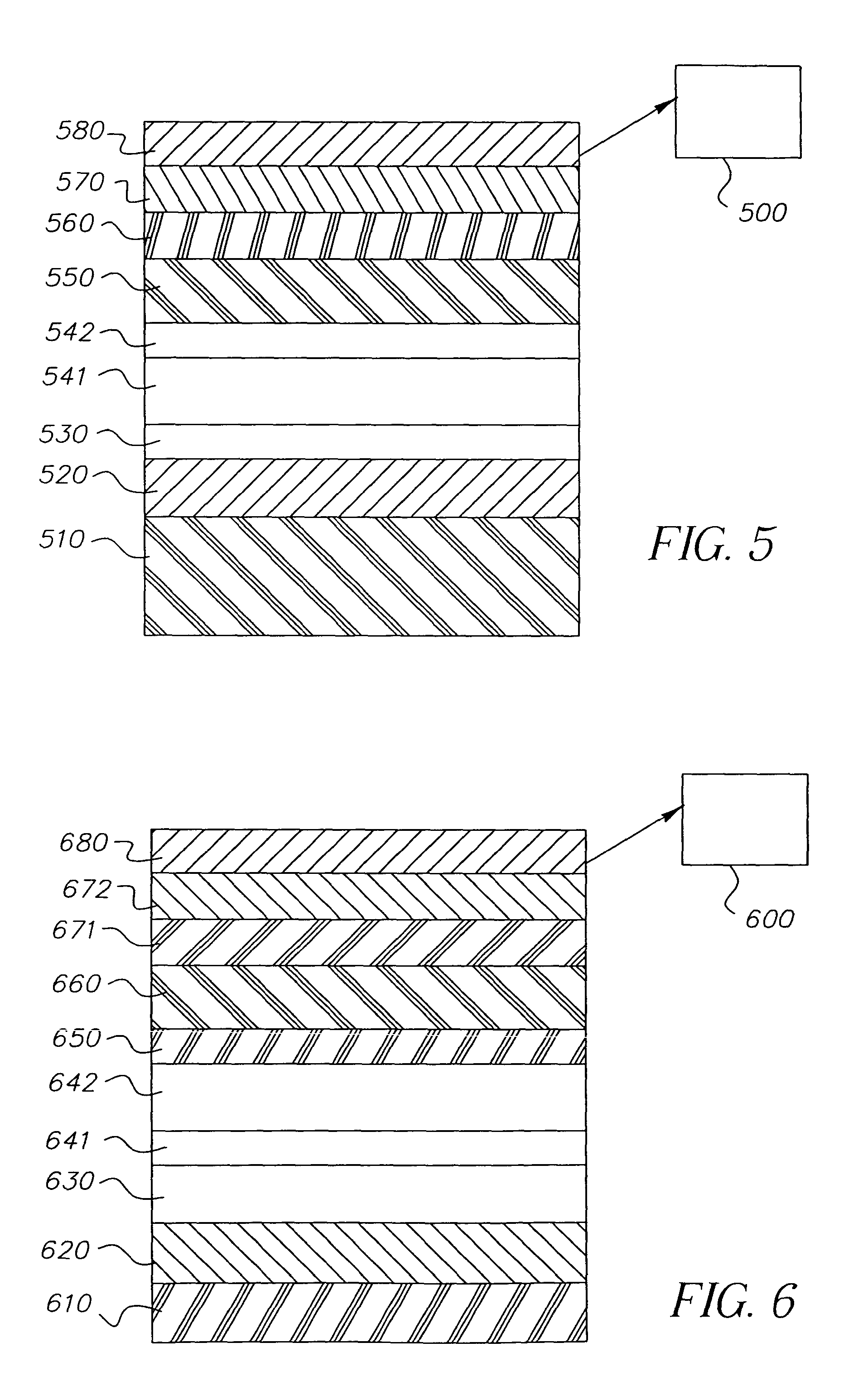
White light-emitting device structures
a technology of light-emitting devices and diodes, which is applied in the direction of discharge tubes luminescnet screens, transportation and packaging, and natural mineral layered products, etc., can solve the problems of difficult manufacturing, difficult control, and only transmitting about 30% of the original white light, and achieve high reproducibility, high efficiency, and high operational stability
- Summary
- Abstract
- Description
- Claims
- Application Information
AI Technical Summary
Problems solved by technology
Method used
Image

Examples
examples
[0136]The invention and its advantages are illustrated by the examples that follow. The term “percentage” indicates the percentage by volume as measured using thin-film deposition monitors of a particular dopant relative to the host material. The procedure for fabrication of all of the OLEDs described hereinafter is illustrated for the case of comparative Example 1. The current-voltage characteristics of each OLED were evaluated using a constant-current source-meter. The electroluminescence spectrum and yield were evaluated using the constant-current source and a diode-array spectrometer. The emission was filtered through a red, green, or blue filter and the photometric performance for each color was also measured. For some of the examples, the power consumption of a full-color 2.2″ diagonal OLED display panel was calculated for luminance of 100 cd / m2 at the D6000 white point. The operational stability (device lifetime) was evaluated by operating an OLED at a constant current densit...
PUM
| Property | Measurement | Unit |
|---|---|---|
| thickness | aaaaa | aaaaa |
| thickness | aaaaa | aaaaa |
| thickness | aaaaa | aaaaa |
Abstract
Description
Claims
Application Information
 - R&D Engineer
- R&D Manager
- IP Professional
- Industry Leading Data Capabilities
- Powerful AI technology
- Patent DNA Extraction
Browse by: Latest US Patents, China's latest patents, Technical Efficacy Thesaurus, Application Domain, Technology Topic.
© 2024 PatSnap. All rights reserved.Legal|Privacy policy|Modern Slavery Act Transparency Statement|Sitemap