Optical write apparatus including a plurality of substrates

a write apparatus and substrate technology, applied in the direction of electrographic processes, electrographic processes using charge patterns, instruments, etc., can solve the problems of reducing yield, reducing the size of the apparatus, and emitted diodes, so as to reduce the difference and eliminate the uneven amount of exposure light

Inactive Publication Date: 2006-05-02
RICOH KK
View PDF14 Cites 23 Cited by
  • Summary
  • Abstract
  • Description
  • Claims
  • Application Information

AI Technical Summary

Benefits of technology

[0019]when there is a difference between a reference gap between the light emitting diodes and an actual gap between the light emitting diodes located at the ends of write ranges of the light emitting diodes array units connected at the seam portion, shifting the write range of at least one of light emitting diode array units connected at the seam portion by the ligh

Problems solved by technology

However, it is costly to produce a 1 m long substrate using light emitting diodes aligned at 400 dpi (a dot pitch of 63.5 μm), because the accuracy needs to be maintained in the entire length of the light emitting diode array unit, the size of the apparatus becomes large, and the yield decreases.
Despite the above advantages, the optical write apparatus having a plurality of substrates shifted from each other in the aligning direction of the light emitting diodes has a problem in the dot sw

Method used


Image

  • Optical write apparatus including a plurality of substrates
  • Optical write apparatus including a plurality of substrates
  • Optical write apparatus including a plurality of substrates

Examples


first embodiment

[1] First Embodiment

1-a: Example 1

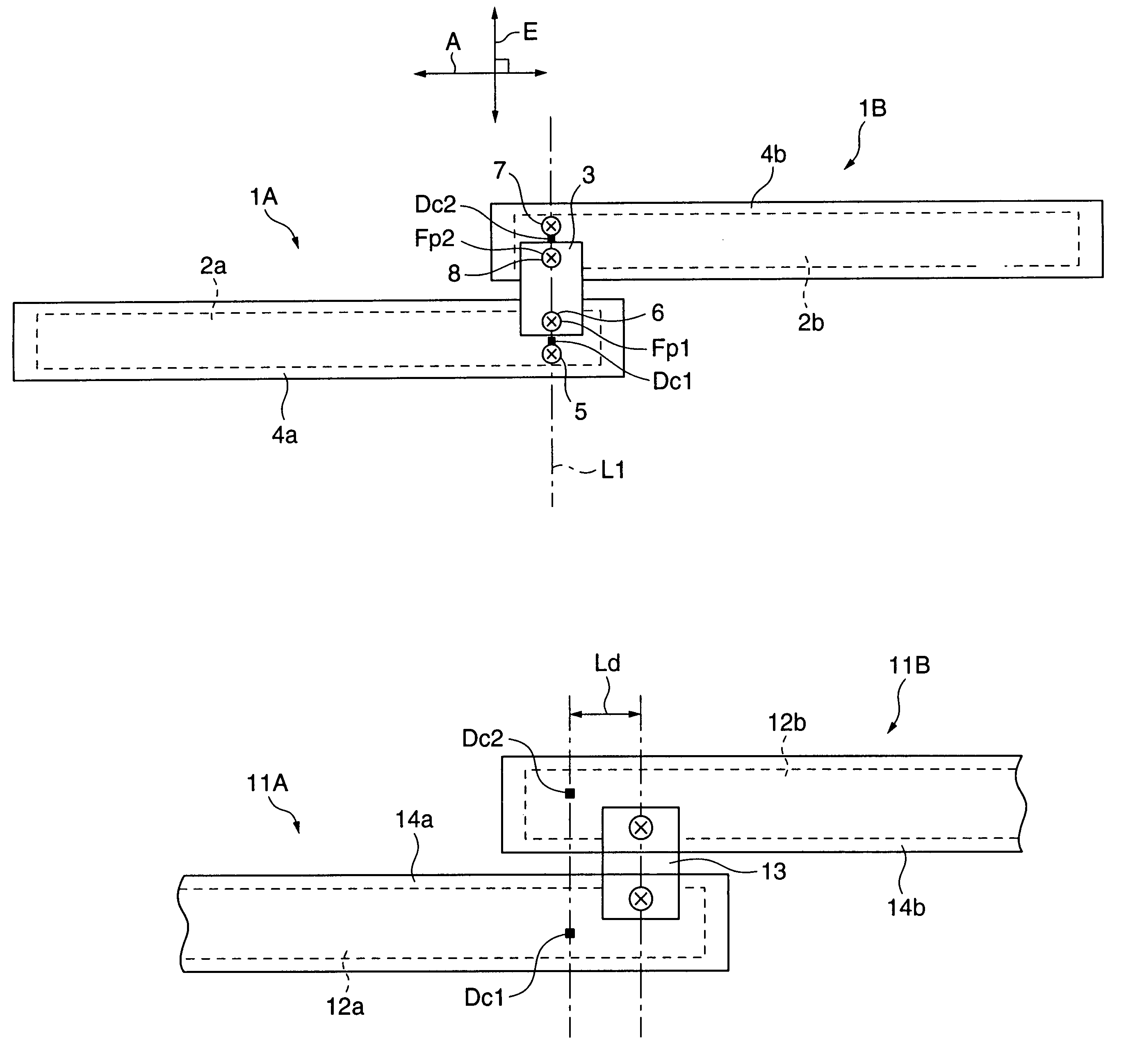
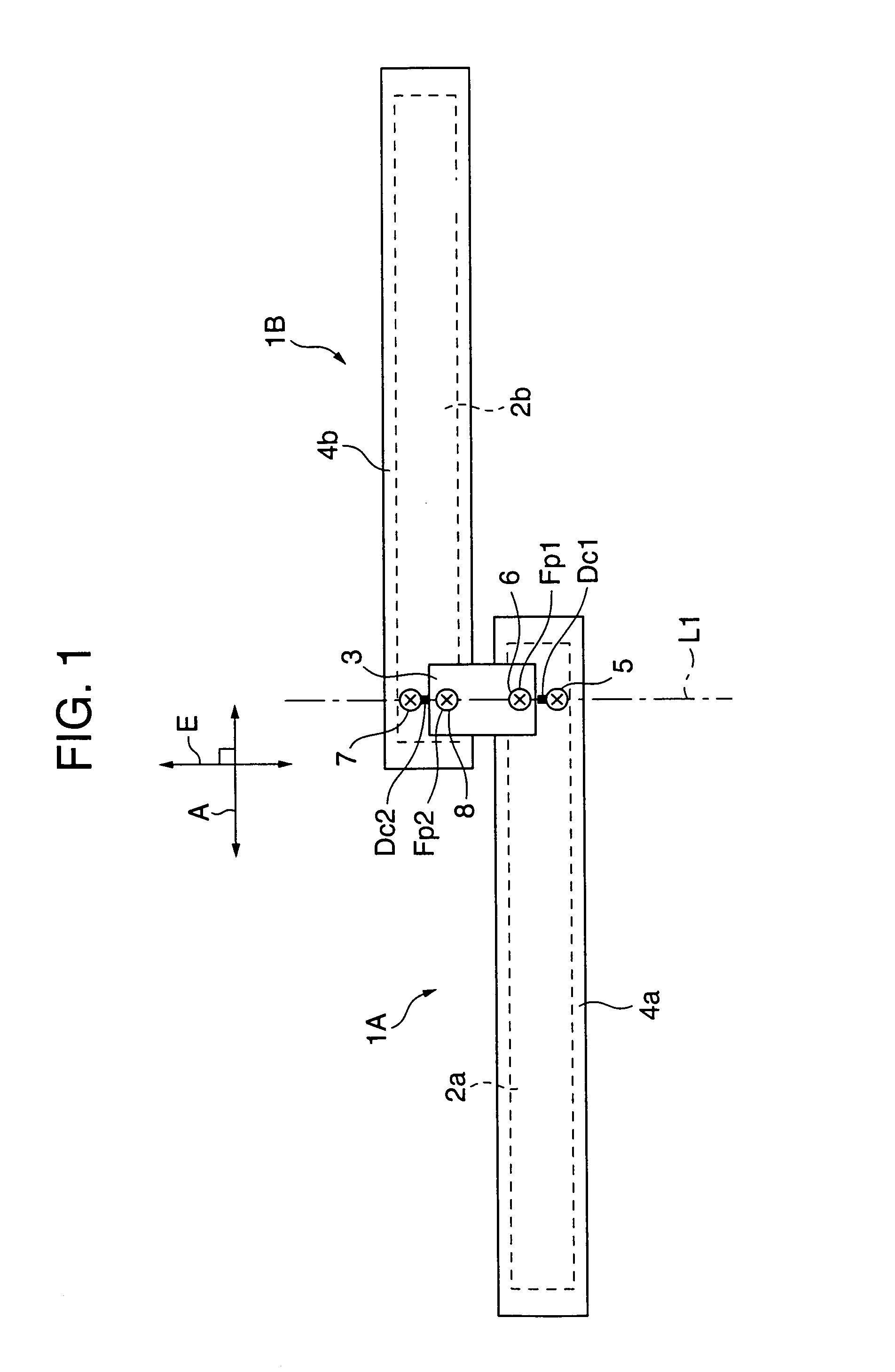
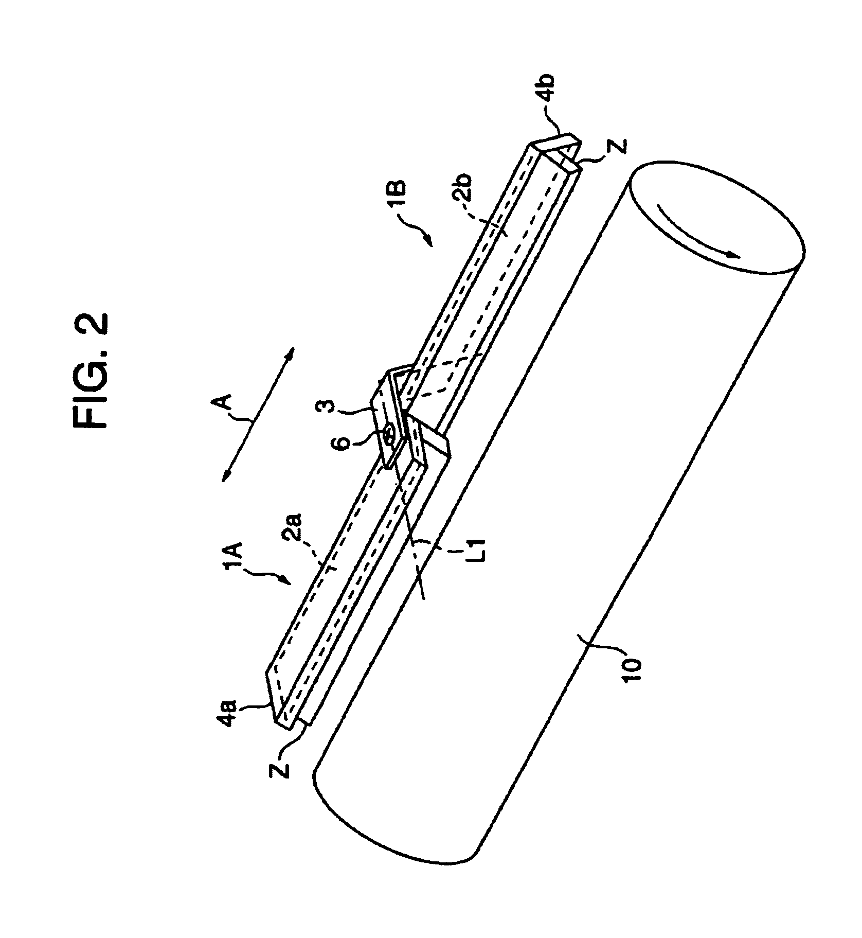
[0063]FIG. 1 is a plan view illustrating the relative positional relationship among a plurality of light emitting diode array units of an optical write apparatus in accordance with the present invention. FIG. 2 is a perspective view of the optical write apparatus and a photosensitive drum in an image forming apparatus.

[0064]This optical write apparatus comprises two light emitting diode array units 1A and 1B having substrates 2a and 2b, respectively, on which a plurality of light emitting diodes (not shown) are arranged in the direction of the arrow A. The light emitting diode array units 1A and 1B are shifted from each other in the direction of the arrow A, and are connected by a connecting member 3, as shown in FIG. 1.

[0065]In this optical write apparatus, dot switching points Dc1 and Dc2 on the substrates of the respective light emitting diode array units 1A and 1B, a fixing point Fp1 for fixing the connecting member 3 to the light emitting diode...

second embodiment

[2] Second Embodiment

2-a: Example 1

[0123]In the first embodiment of the present invention, neighboring substrates are directly fixed to each other, or if an auxiliary member is interposed between two substrates, the fixed positions of the auxiliary member and the substrates are aligned on one line that is perpendicular to the aligning direction of the light emitting diodes. The write dot switching points on the substrates are also located on the same line as the fixed positions.

[0124]In the above optical write apparatus shown in FIG. 1, the light emitting diode array units adjacent to one anther in the direction of the arrow A are fixed to each other via the connecting member 3 at the dot switching points on the substrates. Accordingly, the light from the substrate 2a and the light from the substrate 2b are positioned for writing by varying the write times.

[0125]More specifically, after a line is written by the light emitting diode array unit 1A shown in FIG. 2, the photosensitive d...

third embodiment

[3] Third Embodiment

3-a: Example 1

[0168]In a structure shown in FIG. 3, for instance, after the light emitting diode array unit 1A or 1C draws a line, the photosensitive drum 10 rotates for a predetermined period of delay time, and the light emitting diode array unit 1B then draws a line. In this manner, one horizontal line is drawn.

[0169]The above delay time is normally fixed because of the structure of a write control device. In that case, the write dot distance on the photosensitive member between the light emitting diode array units needs to be accurately adjusted. In reality, however, the write dot distance varies greatly on the photosensitive member, due to an error in component size or assembling of the optical write apparatus. The variation of the write dot distance results in seams in the vertical write direction.

[0170]The delay time can be controlled, but a control device for controlling the delay time is complicated, and the controlling is carried out only by 1 dot (63.5 ...


PUM


Abstract

An optical write apparatus includes a plurality of substrates each having a large number of light emitting diodes aligned in one direction. Every two adjacent substrates are shifted from each other in the aligning direction of the light emitting diodes, and are fixed to each other directly or via a connecting member.

Description

BACKGROUND OF THE INVENTION[0001]1. Field of the Invention[0002]The present invention relates to an optical write apparatus, a method of adjusting the position of the optical write apparatus, a method of controlling the light emitting condition of the optical write apparatus, and an image forming apparatus.[0003]2. Description of the Related Art[0004]Japanese Laid-Open Patent Application No. 7-61035 (A) and Japanese Patent Publication No. 64-16342 (B) disclose optical write apparatuses comprising a plurality of printed boards (hereinafter referred to simply as “substrates”) each having a great number of light emitting diodes aligned in one direction. Those substrates are shifted from each other in the aligning direction of the light emitting diodes.[0005]In the above prior art, light emitting diode array units include the substrates that are relatively small in length, having a length of A3 size paper (297×420 mm paper), for instance. The light emitting diode array units are arrange...

Claims


Application Information

Patent Timeline
IPC IPC(8): B41J2/45B41J2/385G06K15/22
CPCG06K15/225B41J2/45
Inventor HIYOSHI, TAKAYUKI
Owner RICOH KK
Why Eureka
Try Eureka