Composite intermetal dielectric structure including low-k dielectric material

a dielectric structure and intermetal technology, applied in the direction of basic electric elements, electrical apparatus, semiconductor devices, etc., can solve the problems of limiting the operating speed of semiconductor devices, delay in switching, and incompatibility of many low-k dielectric materials having desirable electrical properties with other adjacent materials and/or processes used

Inactive Publication Date: 2006-05-09
INFINEON TECH AG
View PDF11 Cites 6 Cited by
  • Summary
  • Abstract
  • Description
  • Claims
  • Application Information

AI Technical Summary

Benefits of technology

[0010]The problems and needs outlined above are addressed by the present invention. In accordance with one aspect of the present invention, a method of forming a composite intermetal dielectric structure is provided. This method includes the following steps, the order of which may vary. An initial intermetal dielectric structure is provided, which includes a first dielectric layer and two conducting lines. The two conducting lines are located in the first dielectric layer. A portion of the first dielectric layer is removed between the conducting lines to form a trench. The trench is filled with a second dielectric material. The second dielectric material is a low-k dielectric having a dielectric constant less than that of the first dielectric layer.
[0011]The initial intermetal dielectric structure may further include a liner layer formed between each of the conducting lines and the first dielectric layer, and the trench may be formed between the liner layers. The initial intermetal dielectric structure may further include a hard mask layer atop the first dielectric layer, and the removing of the first dielectric layer portion may include removing a portion of the hard mask layer to form the trench. A cap layer may be formed over the second dielectric material. The second dielectric material may be etched so that it is recessed relative to the conducting lines, a cap layer may be formed over the second dielectric material, and the cap layer may be planarized to be substantially coplanar with the conducting lines. The first dielectric layer is preferably made from a low-k dielectric material. A cap layer may be formed over the composite intermetal dielectric structure. The second dielectric material may or may not be compatible with the process(es) for depositing the conductive lines, the process(es) for planarizing the conducting lines. The second dielectric material may be porous. The first dielectric layer is preferably made from a material having a mechanical strength greater than that of the second dielectric material.
[0012]In accordance with another aspect of the present invention, a method of fabricating a semiconductor device is provided. This method includes the following steps, the order of which may vary. A first dielectric layer is formed. Openings are formed in the first dielectric layer using a damascene process. The openings are filled with conductive material to form conducting lines and / or vias. A chemical mechanical polish (CMP) is performed to remove excess conductive material (if any) and to provide a substantially planar upper surface. Select portions of the first dielectric layer are patterned and etched away between at least two conducting lines to form trenches. A second dielectric material is formed in the trenches. The second dielectric material is a low-k dielectric material having a dielectric constant value less than that of the first dielectric layer. The conductive material may include copper, for example. The first dielectric layer is preferably a low-k dielectric material.
[0013]In accordance with yet another aspect of the present invention, a method of fabricating a semiconductor device is provided. A blanket layer of conductive material is formed. Conductive lines are formed in the conductive material layer. A first dielectric layer is formed between and beside the conductive lines. Select portions of the first dielectric layer are patterned and etched away between at least two conducting lines to form trenches. A second dielectric material is deposited in the trenches. The second dielectric material is a low-k dielectric material having a dielectric constant value less than that of the first dielectric layer. The conductive material may include aluminum, for example. The first dielectric layer is preferably a low-k dielectric material.

Problems solved by technology

The RC delay in switching is one factor that limits the operating speed of semiconductor devices.
Also, many low-k dielectric materials having desirable electrical properties may be incompatible with other adjacent materials and / or processes used to form or process such adjacent materials.
Because there are so many compatibility issues to consider when trying to implement, introduce, or test a new low-k dielectric material into a conventional intermetal dielectric structure 20 (see e.g., FIG. 1), the complexity, time, and cost of developing and testing new low-k dielectrics can be quite large.

Method used


Image

  • Composite intermetal dielectric structure including low-k dielectric material
  • Composite intermetal dielectric structure including low-k dielectric material
  • Composite intermetal dielectric structure including low-k dielectric material

Examples


Embodiment Construction

[0024]Referring now to the drawings, wherein like reference numbers are used herein to designate like elements throughout the various views, illustrative embodiments of the present invention are shown and described. The figures are not necessarily drawn to scale, and in some instances the drawings have been exaggerated and / or simplified in places for illustrative purposes only. One of ordinary skill in the art will appreciate the many possible applications and variations of the present invention based on the following illustrative embodiments of the present invention.

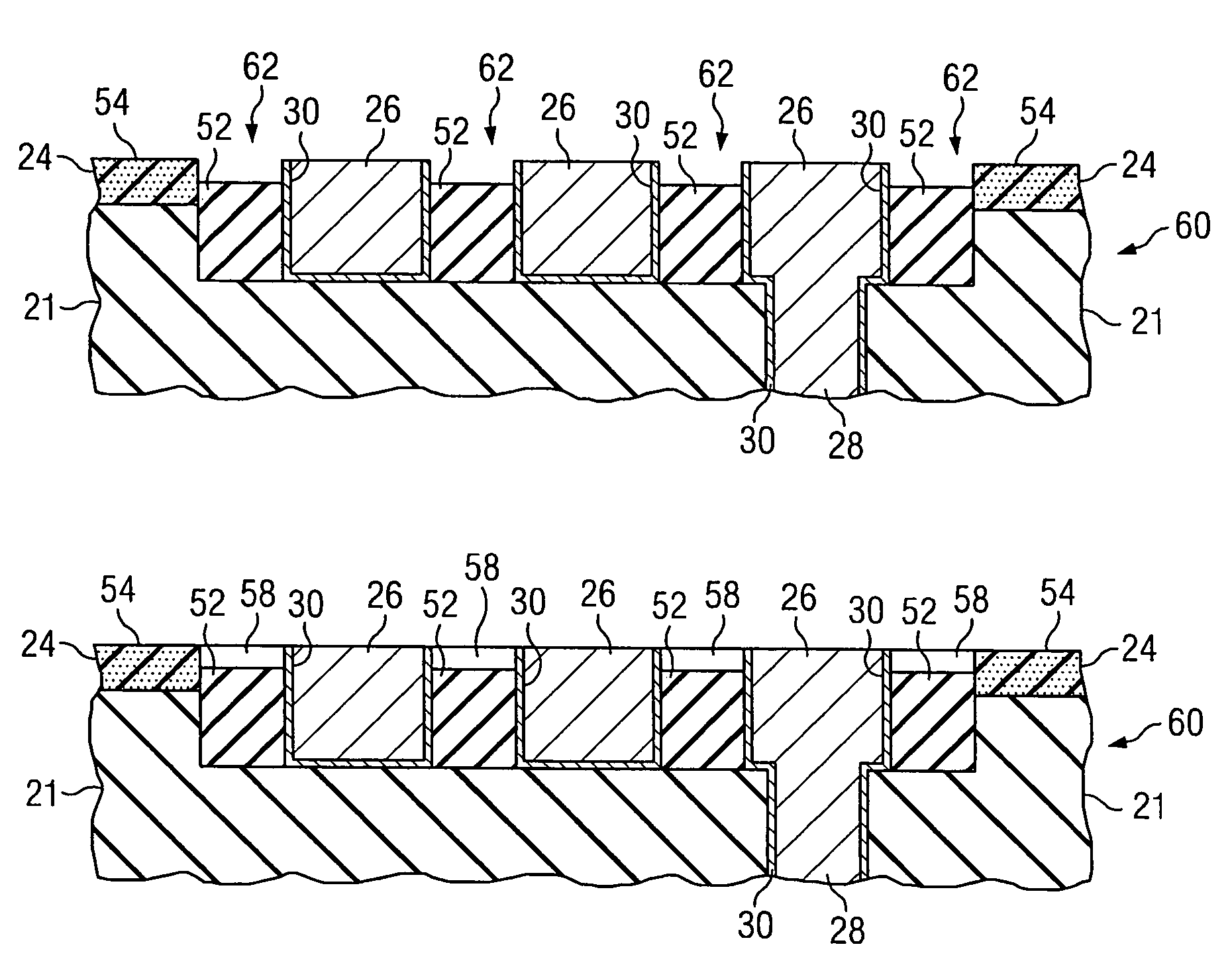
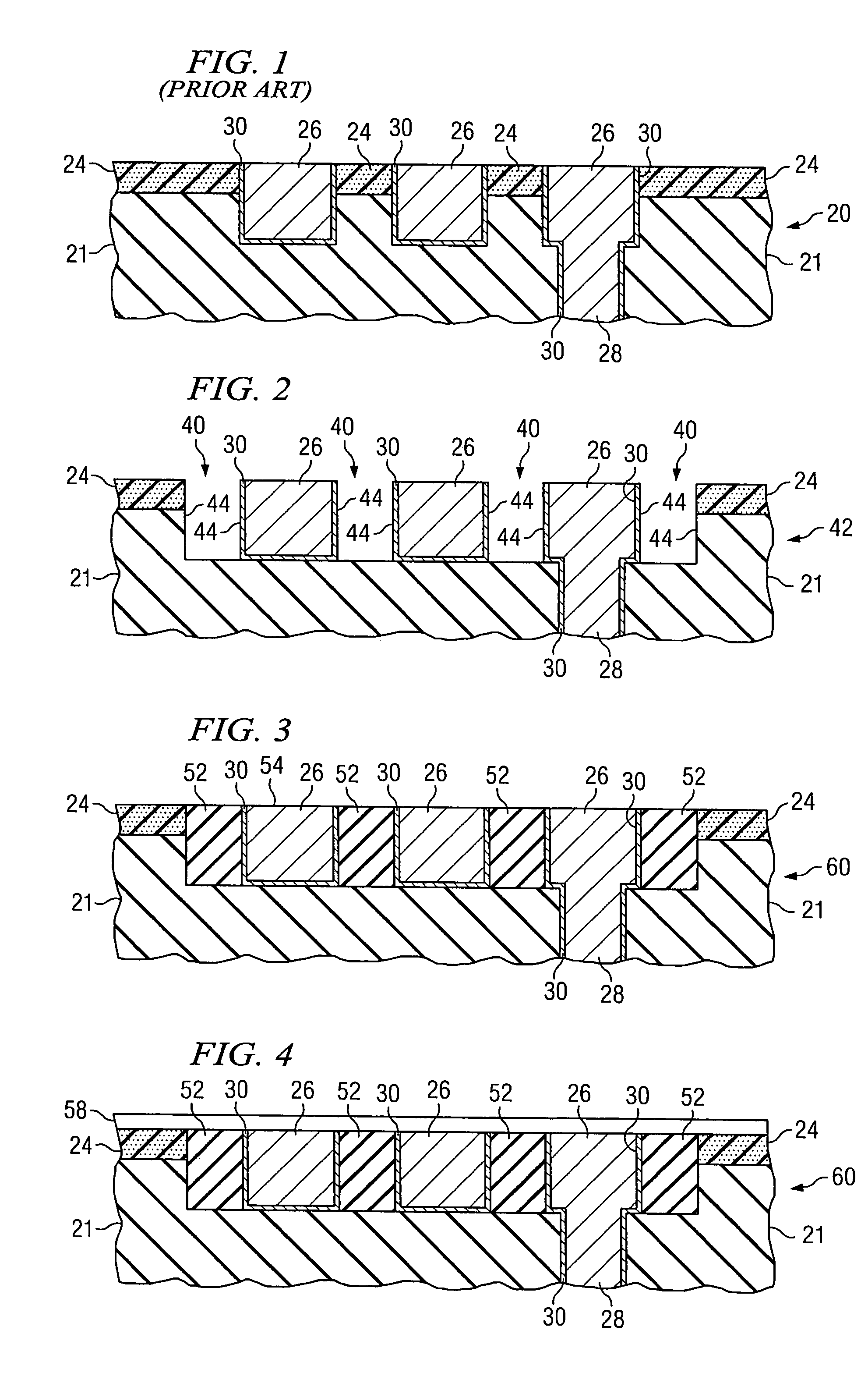
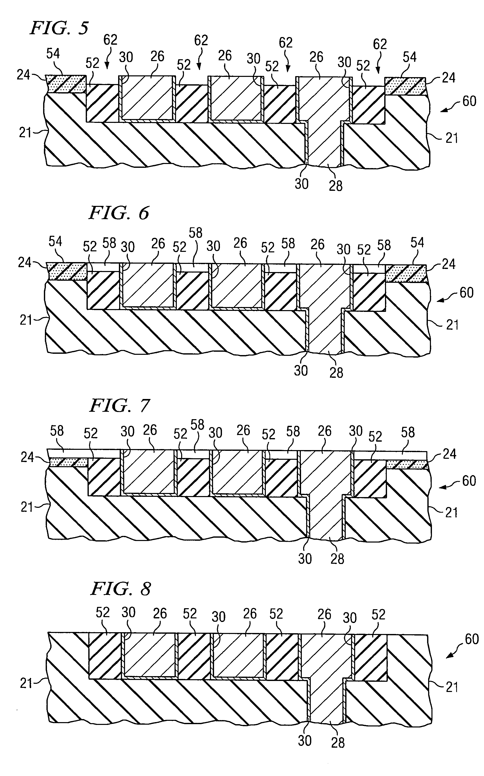
[0025]Generally, an embodiment of the present invention provides a composite low-k structure and methods of fabricating the same. FIGS. 2 and 3 illustrate a method of fabricating a composite low-k magnetic structure in accordance with a first embodiment of the present invention. FIG. 1 is a cross-section view of a portion from a semiconductor device focusing on an intermetal dielectric structure 20. The conventional int...


PUM

PropertyMeasurementUnit
dielectric constantaaaaaaaaaa

Abstract

A method of forming a composite intermetal dielectric structure is provided. An initial intermetal dielectric structure is provided, which includes a first dielectric layer and two conducting lines. The two conducting lines are located in the first dielectric layer. A portion of the first dielectric layer is removed between the conducting lines to form a trench. The trench is filled with a second dielectric material. The second dielectric material is a low-k dielectric having a dielectric constant less than that of the first dielectric layer.

Description

[0001]This application is a continuation of patent application Ser. No. 10 / 457,217, entitled “Composite Intermetal Dielectric Structure Including Low-k Dielectric Material,” filed on Jun. 9, 2003, which application is incorporated herein by reference.FIELD OF THE INVENTION[0002]The present invention relates to fabrication processes and structures for semiconductor devices. In one aspect, it relates to a composite low-k dielectric structure.BACKGROUND[0003]Low-k dielectric materials are dielectric materials having a dielectric constant (k) lower than that of thermal silicon dioxide (i.e., k<3.9). The minimum value of k is 1.0 for air. Hence, Low-k dielectric materials are dielectric material having a dielectric constant between 1.0 and 3.9.[0004]The use of low-k dielectric materials are important in the advancement of integrated circuit applications for semiconductor devices. One advantageous use of low-k materials in semiconductor devices is between conductor lines or structures ...

Claims


Application Information

Patent Timeline
Patent Type & Authority Patents(United States)
IPC IPC(8): H01L21/76H01L21/768
CPCH01L21/76829H01L21/76885H01L21/76835Y10S438/958
Inventor KIM, SUN-OONAUJOK, MARKUSCOWLEY, ANDY
Owner INFINEON TECH AG
Why Eureka
Try Eureka