Providing fluorocarbon layers on conductive electrodes in making electronic devices such as OLED devices

a technology of conductive electrodes and fluorocarbons, which is applied in the direction of basic electric elements, semiconductor devices, electrical equipment, etc., can solve the problems of high resistance of the medium, insufficient hole injection on the bare ito surface, and the operation of the el device requires an extremely high voltage (>100 volts) to achieve the effect of reducing the number of processing stages

Active Publication Date: 2006-05-09
GLOBAL OLED TECH
View PDF24 Cites 40 Cited by
  • Summary
  • Abstract
  • Description
  • Claims
  • Application Information

AI Technical Summary

Benefits of technology

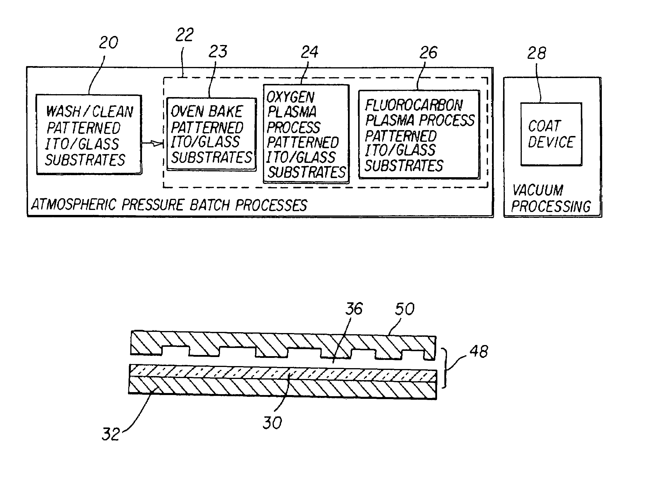
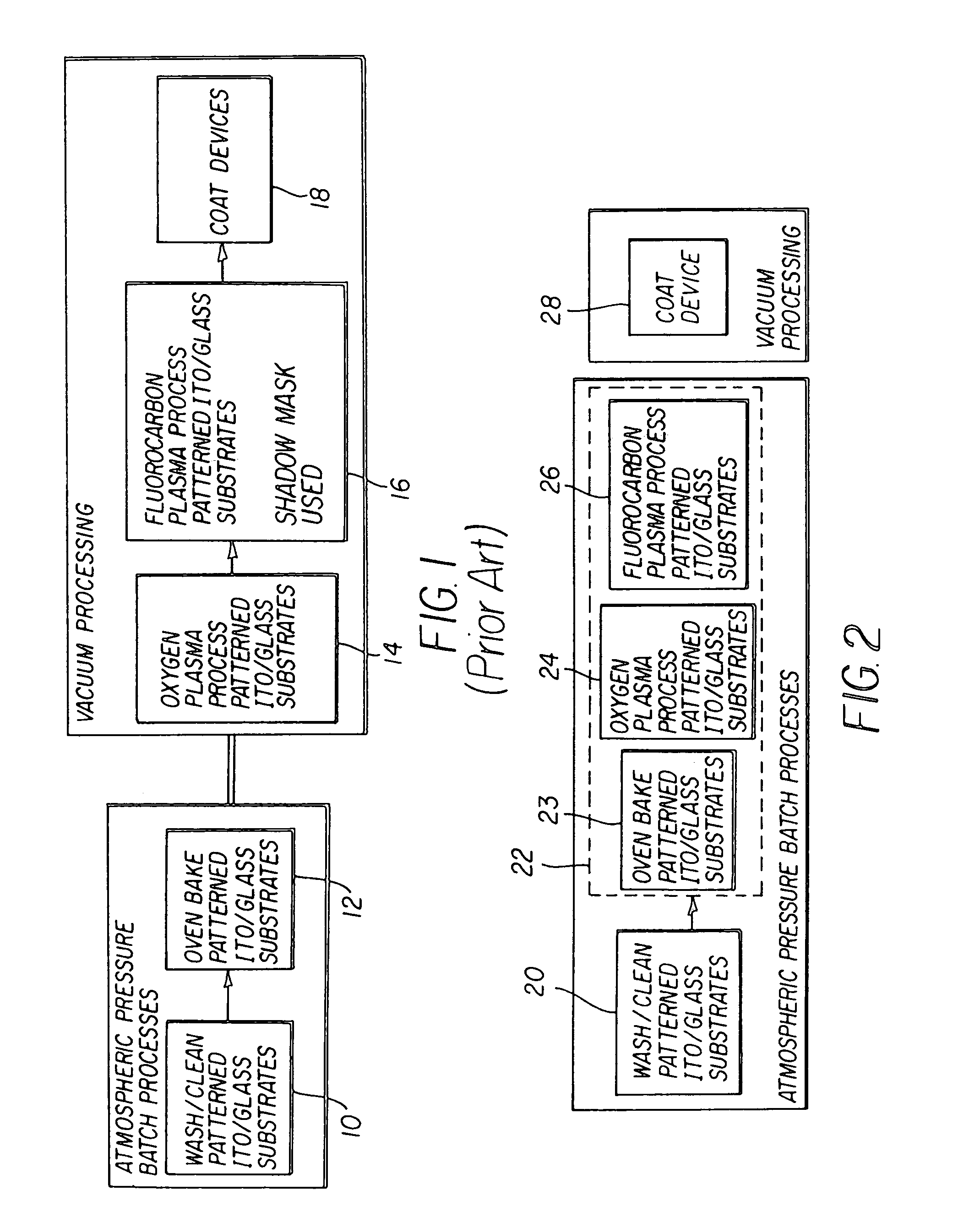
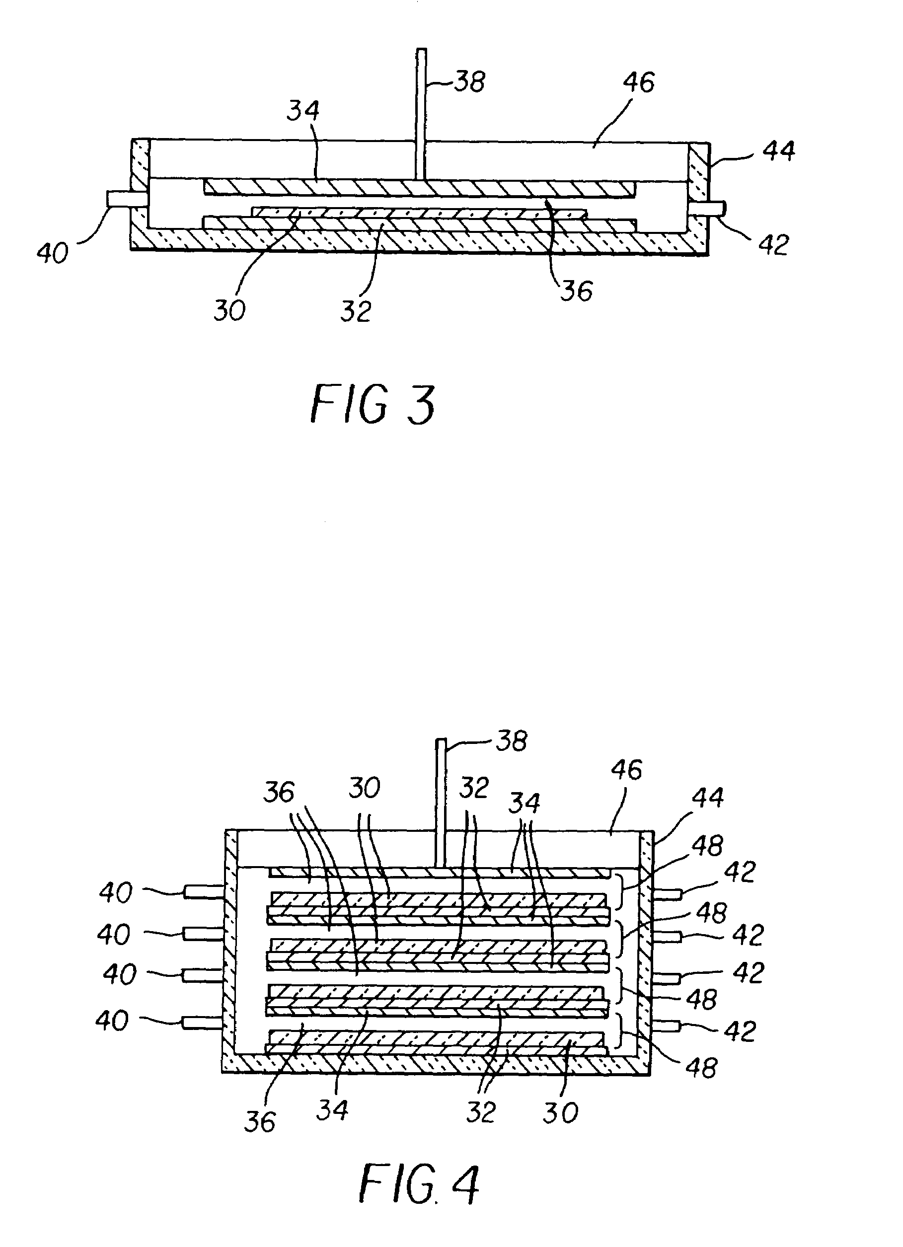
[0019]It is an advantage of the present invention that the process is compatible with oven baking of substrates prior to coating devices, because oven enclosure could be designed with an integral electrode system for carrying out the atmospheric pressure discharge processes for oxygen plasma treatment and fluorocarbon deposition onto the patterned ITO electrodes.
[0020]It is an advantage of the present invention that all steps of the process can be performed at pressures of 0.1 Bar or higher, thus limiting the need for the expensive pumping systems that are normally required for plasma processes.

Problems solved by technology

Thus, this organic EL medium was highly resistive and the EL device required an extremely high voltage (>100 volts) to operate.
However, a device grown on a bare ITO surface generally shows insufficient hole injection and poor operational stability.
The presence of a fluorocarbon film can be detrimental in areas outside the active display area of an OLED flat-panel display, particularly if adhesion of an encapsulating structure to the substrate is necessary.

Method used


Image

  • Providing fluorocarbon layers on conductive electrodes in making electronic devices such as OLED devices
  • Providing fluorocarbon layers on conductive electrodes in making electronic devices such as OLED devices
  • Providing fluorocarbon layers on conductive electrodes in making electronic devices such as OLED devices

Examples


example 1

[0064]Glass substrates 7.6 cm×7.6 cm×1 mm thick were coated with 42 nm of indium tin oxide (ITO) and patterned to produce a set of ITO contacts (4 pairs). The sheet resistance of the ITO is roughly 50 Ohms / sq. The ITO / glass substrates were then cleaned in an ultrasonic bath in deionized water for roughly 10 minutes. The substrates were then spun dry under radiant heat. All samples in this example were vacuum plasma cleaned in a March Asher Model PX250 using flowing oxygen (40 SCCM) at a pressure of 28 Pa and a power of 300 W for 30 seconds. A control sample (A1) was additionally coated with CFx in the March Asher using CHF3 at a flow of 10 SCCM, a pressure of 36 Pa, and a power of 100 W for 10 seconds. A second control sample (A2) was not coated with any CFx. A third sample (A3) was placed in the dielectric barrier discharge cell. A mixture of helium, CF4 and CHF3 was established by flowing 8 slm, 0.1 slm (nominal), and 0.005 slm (nominal) of the respective gases into the discharge ...

example 2

[0067]Another series of samples was prepared similarly to samples A3 and A4 above, except that no vacuum plasma oxygen treatment was carried out prior to dielectric barrier discharge treatment. Instead, a helium oxygen mixture was admitted to the dielectric barrier discharge chamber and discharge treatments were carried out at 30–40 W for the times indicated in Table 2 (samples B1–B4). The oxygen was then shut off, and helium-CF4 or helium-CF4-CHF3 mixtures were established at the flows indicated in Table 2. After purging, a discharge treatment in the fluorocarbon bearing gas mixture was carried out at 30–40 W for 10 seconds. In each case, after all treatments were complete, the chamber was purged with helium and the sample was removed. The light-emitting diode devices thus made were then characterized with respect to light emission, current-voltage characteristics, and lifetime. Additional samples made with substantially lower oxygen flows (0.01 slm) during helium-oxygen discharge ...

example 3

[0069]Yet another series of samples was prepared similarly to samples B1–B4 above, except that a single dielectric barrier discharge process was used to perform simultaneous oxygen and CFx treatment. A helium-oxygen-fluorocarbon mixture (indicated in Table 3 for samples C1–C3) was admitted to the dielectric barrier discharge chamber, and discharge treatments were carried out at 25–30 W for 10 seconds. In each case, after all treatment was complete, the chamber was purged with helium and the sample was removed. As can be seen in Table 3, using the single dielectric barrier discharge process with both oxygen and fluorocarbon present resulted in improved device lifetime relative to the control sample (A2) having no CFx. Furthermore, samples C1–C3 had comparable luminance and drive voltage to the samples produced using vacuum plasma treatments.

[0070]

TABLE 3CFx / Oxygentreatment Gas FlowsCHF3CF4Driverelative lifetimeInitial Luminance(nominal(nominalVoltage @(normalized to(cd / m2) @SampleDes...


PUM


Abstract

A method of making an electronic device in which a conductive electrode has been formed over a substrate including using a liquid to clean the conductive electrode, heating in a processing station the conductive electrode to a temperature which dries the conductive electrode and thereby removes residual cleaning liquid applied during the cleaning step, and providing an oxidizing plasma in the processing station to modify the properties of the conductive electrode. The method also includes producing a fluorocarbon plasma in the processing station to form a fluorocarbon layer over the modified conductive electrode, and further processing the structure to produce the electronic device.

Description

FIELD OF THE INVENTION[0001]This invention relates generally to the manufacture of display devices and, more particularly, to forming a fluorocarbon layer on a conductive electrode of an electronic device such as an OLED device.BACKGROUND OF THE INVENTION[0002]Organic EL devices are known to be highly efficient and are capable of producing a wide range of colors. Useful applications such as flat-panel displays have been contemplated. Representative of earlier organic EL devices are Gurnee et al. U.S. Pat. No. 3,172,862, Gurnee U.S. Pat. No. 3,173,050, and Dresner U.S. Pat. No. 3,710,167. Typical organic emitting materials were formed of a conjugated organic host material and a conjugated organic activating agent having condensed benzene rings. The organic emitting material was present as a single layer medium having a thickness significantly greater than 1 micrometer. Thus, this organic EL medium was highly resistive and the EL device required an extremely high voltage (>100 volt...

Claims


Application Information

Patent Timeline
Patent Type & Authority Patents(United States)
IPC IPC(8): H01L21/31H01L21/44H01L21/302H01L21/312H01L21/316H01L21/461H01L21/768H01L51/50H01L51/52
CPCH01L51/5206H01L51/5088H01L51/0021H01L21/3127H01L21/31683H01L21/0212H10K71/60H10K50/17H10K50/81H10K71/00
Inventor SIEBER, KURT D.GRACE, JEREMY M.HEINSLER, MICHAEL J.SPINDLER, JEFFREY P.
Owner GLOBAL OLED TECH
Why Eureka
Try Eureka