Chip light emitting diode and fabrication method thereof

a light-emitting diode and chip technology, applied in the direction of basic electric elements, electrical equipment, semiconductor devices, etc., can solve the problems of limited optical paths of emitted light rays, high manufacturing cost in some applications, narrow viewing angle of chip leds, etc., to prevent centralization of stress, prevent thermal and mechanical deformation, and simple metal mold structure

Active Publication Date: 2006-05-09
SEOUL SEMICONDUCTOR
View PDF7 Cites 10 Cited by
  • Summary
  • Abstract
  • Description
  • Claims
  • Application Information

AI Technical Summary

Benefits of technology

[0011]It is another object of the present invention to provide a chip LED in which the heat generated is distributed uniformly to avoid thermal and mechanical deformation and to prevent stress from centralizing on one side.
[0012]It is still another object of the present invention to provide a fabrication method of a chip LED, in which a simple metal mold structure can be employed to reduce fabrication costs.

Problems solved by technology

The conventional chip LED 50 has drawbacks in that optical paths of emitted light rays are limited because the resin package 56 has a rectangular cross section, causing a narrow viewing angle of the chip LED.
Therefore, many chip LEDs are required to light a certain area, resulting in high manufacturing cost in some applications such as for backlighting.
Further, heat generated from the conventional chip LED 50 during operation is concentrated in the edges, resulting in thermal or mechanical deformation of the diode.
When the thickness of the resin package is reduced for overall compactness of the conventional chip LED, a metal mold of the resin package should be more precisely formed for the edges, which may result in high manufacturing costs.
Further, when the thickness of the resin package happens to be not uniform, stress may be concentrated at a thin part, so the adhesive strength is deteriorated causing poor reliability of the chip LED.

Method used


Image

  • Chip light emitting diode and fabrication method thereof
  • Chip light emitting diode and fabrication method thereof
  • Chip light emitting diode and fabrication method thereof

Examples


Embodiment Construction

[0035]The present invention will be described in detail with reference to the accompanying drawings.

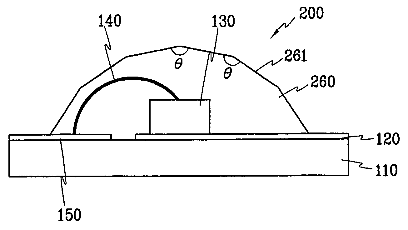
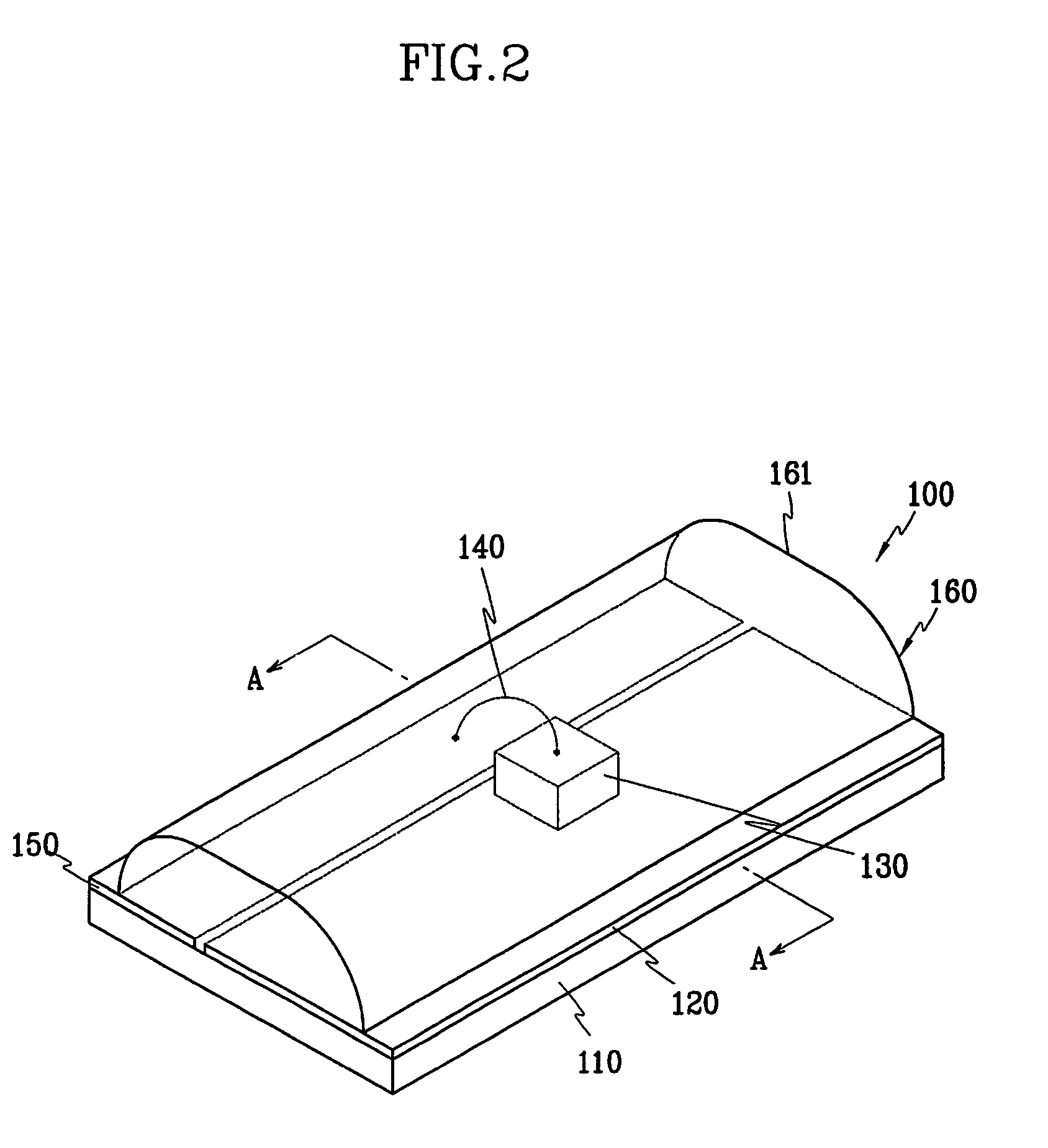
[0036]Referring to FIGS. 2 and 3, a chip light emitting diode (LED) 100 according to a first preferred embodiment of the present invention has a metal pad 120 and a lead 150 provided on a printed circuit board (PCB) 110, and a light emitting chip 130 mounted on the metal pad 120. The metal pad 120 is made of an electrically conductive material, and the chip 130 may be suitably selected from among light emitting chips of wavelengths ranging from infrared to ultraviolet. A wire 140 connects the light emitting chip 130 to the lead 150, and a resin package is formed protruding from the PCB 110 to seal the chip 130 and parts of the lead 150 and metal pad 120.

[0037]The resin package 160 has a curved projecting part 161 which has a cross section that is substantially semicircular. The cross section is elongated to form a cylindrical outer surface of the resin package 160. A suitable epoxy re...


PUM


Abstract

A chip light emitting diode having a wide viewing angle, and a fabrication method thereof. The chip light emitting diode has a resin package sealing a light emitting chip which has at least one curved projecting part. The curved projecting part has a cross section which is substantially semicircular, or substantially or partially elliptical or parabolic. The curved projecting part preferably has a cross section which is comprised of a plurality of straight lines, an angle being formed between adjacent lines. The cross section is elongated to form a cylindrical outer surface of the resin package.

Description

BACKGROUND OF THE INVENTION[0001](a) Field of the Invention[0002]The present invention relates to a chip light emitting diode and a fabrication method thereof.[0003](b) Description of the Related Art[0004]Chip light emitting diodes (LEDs) are generally employed as display devices and for backlighting. Recently, their use range has been increased to include various applications such as light sources for mobile phones and personal digital assistants (PDAs).[0005]Referring to FIG. 1, a conventional chip LED 50 is provided with a metal pad 52 and a lead 55 on a printed circuit board (PCB) 51. A light emitting chip 53 mounted on the metal pad 52 is connected to the lead 55 via a wire 54. A resin package 56 is formed of an epoxy mold compound (EMC), and seals the chip 53.[0006]The conventional chip LED 50 has drawbacks in that optical paths of emitted light rays are limited because the resin package 56 has a rectangular cross section, causing a narrow viewing angle of the chip LED. Furthe...

Claims


Application Information

Patent Timeline
Patent Type & Authority Patents(United States)
IPC IPC(8): H01L29/22H01L27/15H01L33/56H01L33/54H01L33/62H01L33/64
CPCH01L33/54H01L33/486H01L2924/1815H01L2224/48091H01L2924/00014
Inventor HAN, KWAN-YOUNGKIM, DO-HYUNGYANG, SEUNG-MANLEE, CHUNG-HOONKIM, HONG-SANPARK, KWANG-IL
Owner SEOUL SEMICONDUCTOR
Why Eureka
Try Eureka