Nonvolatile semiconductor memory device comprising a variable resistive element containing a perovskite-type crystal structure

a semiconductor memory and variable resistive element technology, applied in semiconductor devices, digital storage, instruments, etc., can solve the problems of high cost and destructive reading, inferior micronization and high-speed operation of ferromagnetic tunnel effect elements, and inferior micronization and high-speed operation since thermal operation. , to achieve the effect of increasing reducing the substantially effective contact area, and reducing the resistance of the variable resistor

Active Publication Date: 2006-05-16
XENOGENIC DEV LLC
View PDF3 Cites 85 Cited by
  • Summary
  • Abstract
  • Description
  • Claims
  • Application Information

AI Technical Summary

Benefits of technology

[0011]According to the nonvolatile semiconductor memory device of the present invention, the particulate electrode does not have a uniform flat surface, but has a minutely irregular surface depending on each particle diameter of the particulate conductors. Therefore, on the interface with the variable resistor, the whole surface of the particulate electrode is not electrically in contact but many points on the surface of the particulate electrode are in contact, enabling a great reduction in substantially effective contact area while the contact area remains unchanged. Further, the knowledge newly discovered by the present inventors confirms that the resistance of the variable resistor with the perovskite-type crystal structure increases when the contact area with the electrode becomes smaller even if the cross-sectional area thereof remains unchanged. Namely, in the variable resistor, a current that flows through the contact portion along the voltage-applying direction is considered as exclusively contributing to the resistance, whereas a current that flows in the lateral direction (direction vertical to voltage-applying direction) is considered as hardly contributing to the resistance. Therefore, by making at least one of the lower electrode and the upper electrode a particulate electrode, it is possible to increase the resistance of the variable resistor in a low resistance state to a value so high as to be driven by a normally usable pulse power source or pulse application circuit. This also permits free control of the resistance value while the contact cross-sectional area remains unchanged, by suitable selection of particle diameters (or mean particle diameter) of the particulate conductors constituting the particulate electrode. Consequently, it is possible to obtain a variable resistive element with a suitable resistance value irrespective of the variable resistor area or the electrode area, so as to provide a nonvolatile semiconductor memory device capable of programming information irrespective of large current drive.

Problems solved by technology

The FeRAM is superior in low electric power consumption and high-speed operation, but inferior in high cost and destructive reading.
However, the ferromagnetic tunnel effect element has a major problem of high electric power consumption in inversion of magnetization at the time of programming, as well as micronization.
Further, the OUM, which is produced on the basis of thermal phase transformation of a chalcogenide material, is superior in low cost and process matching, but inferior in micronization and high-speed operation since it thermally operates.
Such a high operation voltage is practically problematic.
However, the present inventors have clarified the fact that reduction in thickness of the perovskite thin film in the same element area and the same electrode area causes a very low impedance, a resistance value of 10Ω or less, of the variable resistive element, leading to insufficient capacity to supply current in a commonly usable pulse power source or pulse application circuit.
Thereby application of sufficient voltage to the variable resistive element becomes difficult.

Method used


Image

  • Nonvolatile semiconductor memory device comprising a variable resistive element containing a perovskite-type crystal structure
  • Nonvolatile semiconductor memory device comprising a variable resistive element containing a perovskite-type crystal structure
  • Nonvolatile semiconductor memory device comprising a variable resistive element containing a perovskite-type crystal structure

Examples


Embodiment Construction

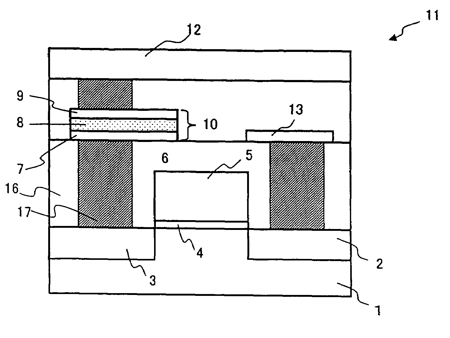
[0026]One embodiment of the nonvolatile semiconductor memory device according to the present invention (hereinafter, appropriately referred to as “the inventive device”) will be described on the basis of drawings.

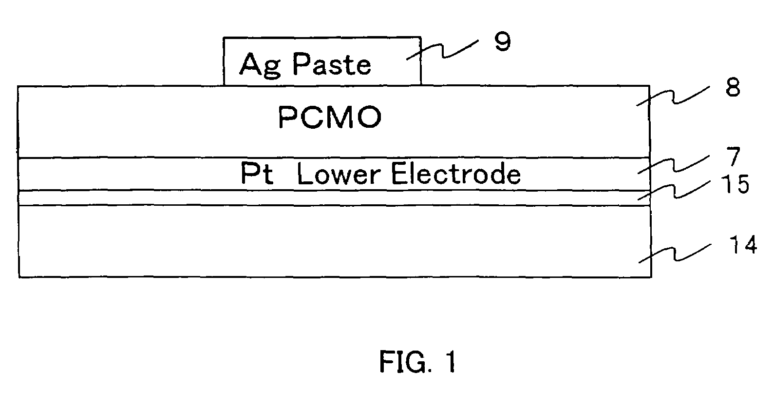
[0027]FIG. 1 is a cross-sectional view illustrating a basic structure of a variable resistive element 10 as a nonvolatile memory element for use in the inventive device 100. The variable resistive element 10 basically has a stack structure formed by sequentially stacking a lower electrode 7, a variable resistor 8 with a perovskite-type crystal structure, and an upper electrode 9. The variable resistive element 10 is further characterized in that the upper electrode 9 is a particulate electrode configured of a particulate conductor aggregate. In the following, the variable resistive element 10 will be described in detail.

[0028]The variable resistive element 10 having the basic structure illustrated in FIG. 1 is formed as follows. First, a TiO2 layer 15 as a barrier contact l...


PUM


Abstract

In a nonvolatile semiconductor memory device including a variable resistive element formed by sequentially stacking a lower electrode, a variable resistor with a perovskite-type crystal structure, and an upper electrode, at least one of the lower electrode and the upper electrode is a particulate electrode configured to include a particulate conductor aggregate so that the contact area with the variable resistor at an interface is effectively reduced to realize high initial resistance of the variable resistive element. Further, a film of the variable resistor is preferably formed so as to be in a highly crystalline state.

Description

CROSS REFERENCE TO RELATED APPLICATION[0001]This Nonprovisional application claims priority under 35 U.S.C. §119(a) on Patent Application No. 2003-405718 filed in Japan on Dec. 4, 2003, the entire contents of which are hereby incorporated by reference.BACKGROUND OF THE INVENTION[0002]1. Field of the Invention[0003]The present invention relates to a nonvolatile semiconductor memory device. More specifically, the present invention relates to a nonvolatile semiconductor memory device including a variable resistive element formed by sequentially stacking a lower electrode, a variable resistor with a perovskite-type crystal structure, and an upper electrode.[0004]2. Description of the Related Art[0005]As next generation nonvolatile random access memories (NVRAM) capable of operating at high speed, that replace flash memories, there have recently been proposed memories with a variety of device structures, such as FeRAM (Ferroelectric RAM), MRAM (Magnetic RAM) and OUM (Ovonic Unified Memor...

Claims


Application Information

Patent Timeline
Patent Type & Authority Patents(United States)
IPC IPC(8): H01L29/76H01L27/10G11C13/00H01L21/8234H01L45/00
CPCG11C13/0007H01L45/1253H01L45/147H01L45/04H01L45/1233H01L45/1625G11C2213/31G11C2213/79H01L27/2436G11C2213/52H10B63/30H10N70/20H10N70/826H10N70/841H10N70/8836H10N70/026
Inventor TAMAI, YUKIOAWAYA, NOBUYOSHIKOBAYASHI, SHINJIKAWAZOE, HIDECHIKASUZUKI, TOSHIMASAMASUDA, HIDETOSHIHAGIWARA, NAOTOMATSUSHITA, YUJINISHI, YUJI
Owner XENOGENIC DEV LLC
Why Eureka
Try Eureka