Motion vector correction circuit and method

Inactive Publication Date: 2006-05-23
SONY CORP
View PDF20 Cites 15 Cited by
  • Summary
  • Abstract
  • Description
  • Claims
  • Application Information

AI Technical Summary

Benefits of technology

[0029]It is therefore an object of the present invention to overcome the above-mentioned drawbacks of the related art by suppressing degradation in quality of a frequenc

Problems solved by technology

Thus, a new field cannot be produced between fields while maintaining the interlaced state.
In such a case, if an image is shifted in blocks by the image shifter 73 in the direction of a motion vector, the motion vector will inaccurately

Method used


Image

  • Motion vector correction circuit and method
  • Motion vector correction circuit and method
  • Motion vector correction circuit and method

Examples


Embodiment Construction

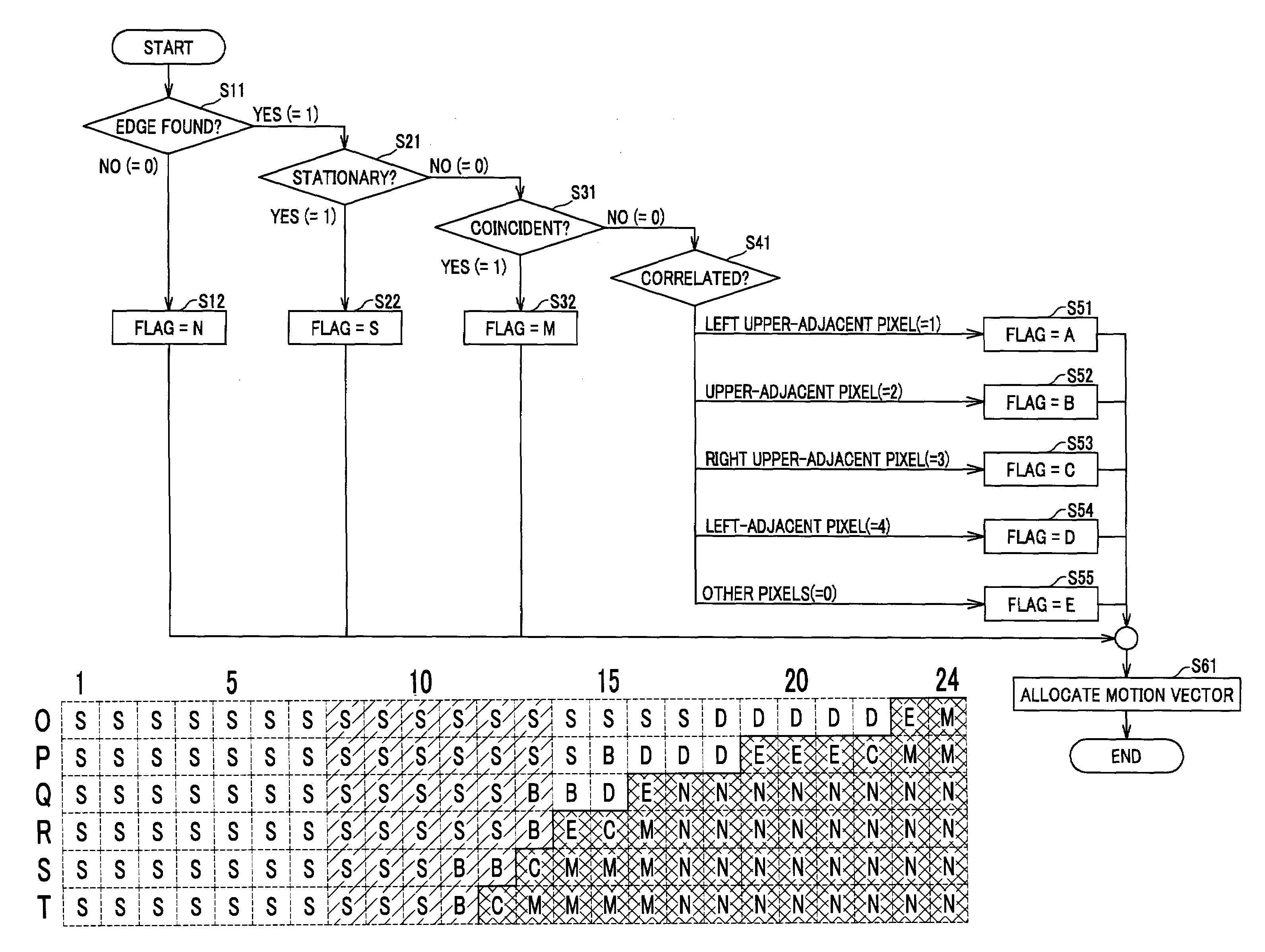
[0063]The embodiment of the present invention will be described herebelow with reference to the accompanying drawings.

[0064]The motion vector correction apparatus according to the present invention is generally indicated with a reference 1. The motion vector correction apparatus 1 is integrally built in a motion correction system 9 used in a TV receiver of, for example, the PAL (phase alternation by line) type.

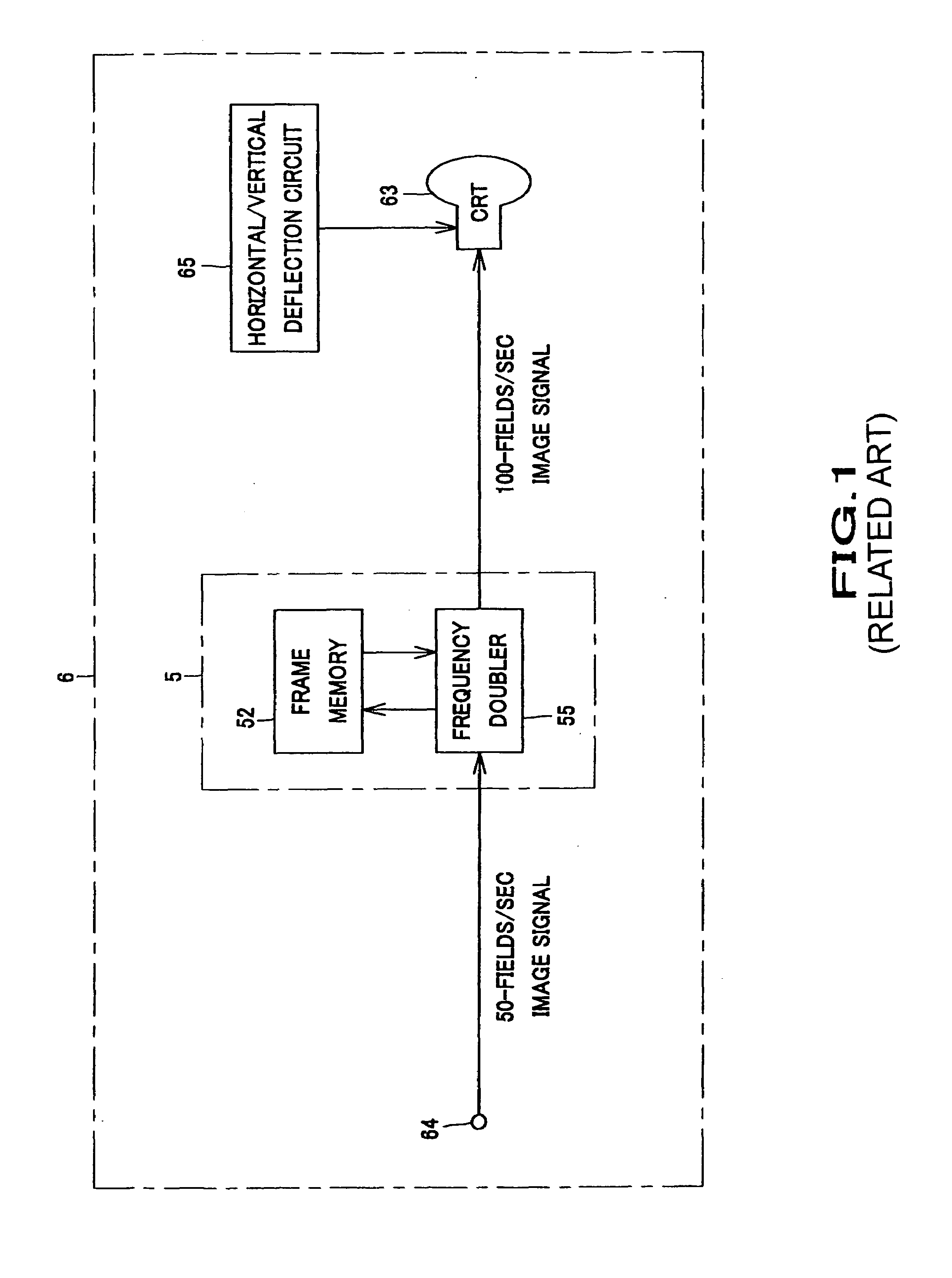
[0065]Referring now to FIG. 7, there is schematically illustrated in the form of a block diagram the motion correction system 9. As shown, the motion correction system 9 includes an image memory 61, image shifter 62 and the motion vector correction apparatus 1 according to the present invention.

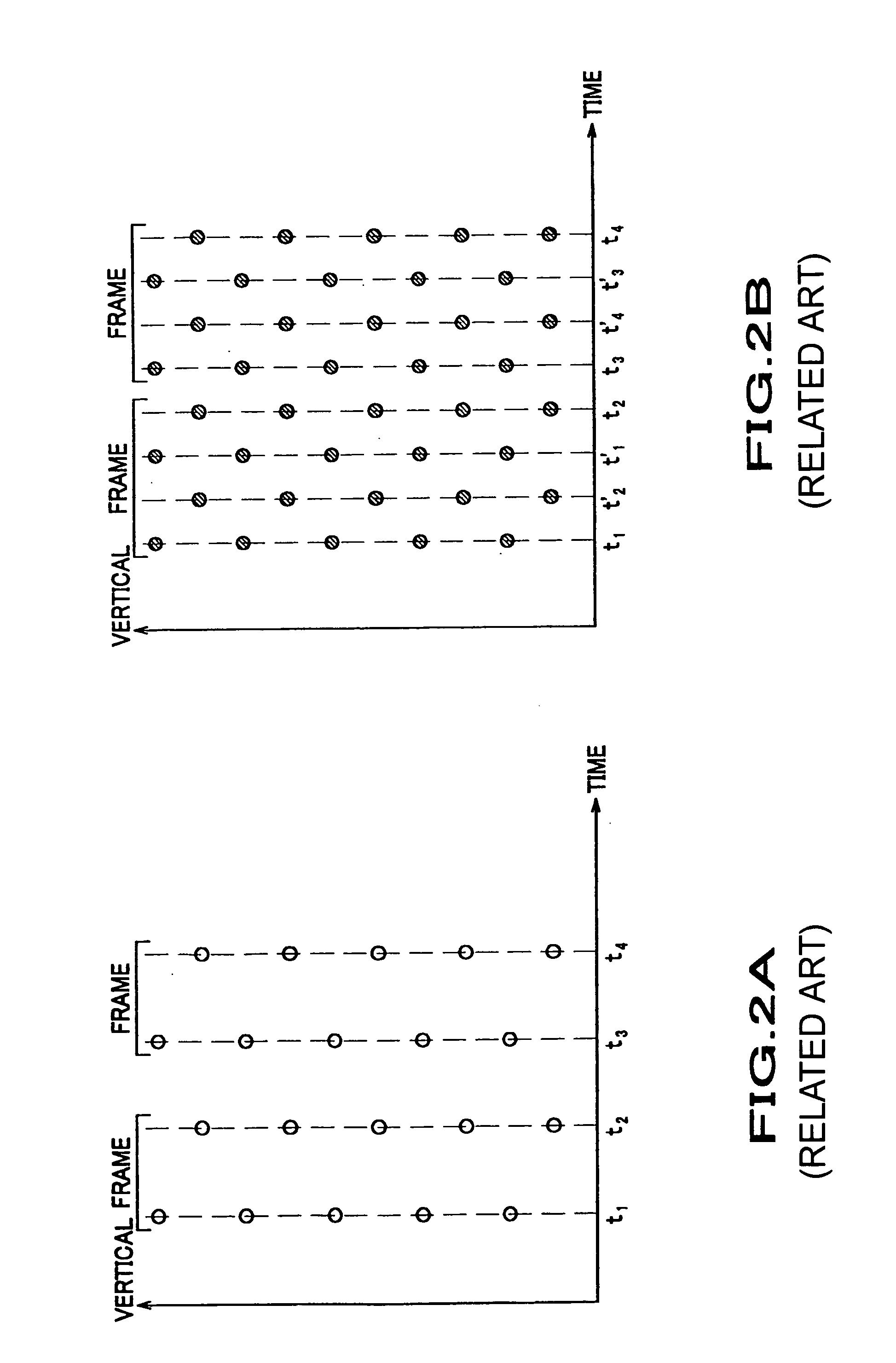
[0066]The above image memory 61 stores sequentially supplied interlaced image signals in units of a field for one frame. In the following explanation, an image signal output from the image memory 61 will be referred to as “basic field”30 hereunder, and an image signal input to the image...


PUM


Abstract

It is determined whether each block (51) including a plurality of pixels extracted from a basic field (30) has an edge or not, and then which state, stationary or non-stationary, each of the pixels forming together the block (51) determined to have an edge is. There is calculated an absolute value of a difference between a pixel determined to be non-stationary and a pixel (91 or 92) in each pixel position in a reference field (40) or pixels (82 to 85) included in the reference field and adjacent to the non-stationary pixel, and a correlation is found between such pixels in consideration according to the calculated difference absolute-value. A motion vector is determined by the block matching method according to results of the determination, and allocated to each of the pixels. Thus, the motion vector of each block is corrected to an accurate one of each of the pixels.

Description

BACKGROUND OF THE INVENTION[0001]1. Field of the Invention[0002]The present invention generally relates to a motion vector correction circuit and method, and more particularly to a circuit for, and a method of, correcting a motion vector determined by the block matching method.[0003]This application claims the priority of the Japanese Patent Application No. 2002-145265 filed on May 20, 2002, the entirety of which is incorporated by reference herein.[0004]2. Description of the Related Art[0005]Heretofore, the TV broadcasting systems have adopted most widely the interlaced scanning or interlacing in which the electron beam is scanned across the screen once every other horizontal scan line. In the interlacing, a field image formed from odd scan lines and a one formed from even scan lines, form together one frame image. An image interlaced with a low frequency incurs a flicker in screen (will be referred to as “screen flicker” hereunder) which will degrade the on-screen image quality.[0...

Claims


Application Information

Patent Timeline
IPC IPC(8): H04N7/01H04N11/20G06T7/20H04N5/14H04N7/12H04N7/36
CPCH04N5/145H04N7/0132H04N19/40H04N19/503H04N19/51H04N19/537H04N5/142H04N7/0112H04N7/0142
Inventor NISHIBORI, KAZUHIKOAOYAMA, KOJIMOGI, YUKIHIKOHOSHINO, TAKAYAKONDO, MAKOTO
Owner SONY CORP
Why Eureka
Try Eureka