Exposure device

a technology of exposure device and core substrate, which is applied in the direction of circuit mask, printing, instruments, etc., can solve the problems of difficult identification of alignment mark on the core substrate, inability to establish alignment technology, and inability to automate manufacturing processes

Inactive Publication Date: 2006-05-23
ADTEC ENG
View PDF5 Cites 7 Cited by
  • Summary
  • Abstract
  • Description
  • Claims
  • Application Information

AI Technical Summary

Benefits of technology

[0012]The present invention was developed in consideration of the above mentioned problems, and an object of the present invention is to provide an exposure device by which aligning of an exposure pattern is realized when manufacturing a build-up structure such as a build up wiring board or the like, and which can cope with automation of manufacturing process.
[0024]In the second aspect of the present invention, the alignment is carried out such that the spatial modulating element which modulates the light beam and the laminated structure are relatively moved by the moving section in the direction so as to be parallel to the surface to be exposed of the photosensitive material. The direction so as to be parallel to the surface to be exposed of the photosensitive material is a direction, for example, a main scanning direction of the light beam (a X direction), a sub scanning direction of the light beam (a Y direction), a rotation direction to which this X-Y coordinate system is rotated, and the like. Namely, the direction parallel to the surface to be exposed of the photosensitive material is one of the directions mentioned above, or combination of a plurality of directions mentioned above. The alignment of the exposure position can be easily realized due to that the an mechanically structured moving section is used as the aligning section mentioned above.
[0025]In the third aspect of the present invention, the control section controls the spatial modulating element to change modulating timing or the like of the light beam on the basis of the control signal generated in accordance with the image information. As the result, exposure alignment is carried out. Even if the aligning section is structured by the electrical control section which changes the modulating timing or the like of the light beam, the exposure pattern alignment can be carried out. Further, the device structure can be more simple compared to a case in which the an mechanically structured moving section is used as the aligning section.

Problems solved by technology

Accordingly, the exposure device has a problem in an alignment (identification of the alignment mark and positioning (aligning) of an exposure pattern) which is carried out after the build up layer is laminated on the core substrate.
However, it is difficult to identify the alignment mark on the core substrate after building up (laminating) of the build up layer by such image-pickuping device using a visible light when manufacturing the build up wiring board.
Therefore, establishment of alignment technology becomes a problem in a case of to using an exposure device which exposes a pattern (an image) with light beam when manufacturing the build up wiring board.
However, manufacturing processes cannot be automated by the method mentioned above, merit to introduce the device fades, and there is a problem that a manufacture cost has risen.

Method used


Image

  • Exposure device
  • Exposure device
  • Exposure device

Examples


Embodiment Construction

[0062]Referring to drawings, an embodiment of the present invention will be described hereinafter in detail.

Structure of Exposure Device

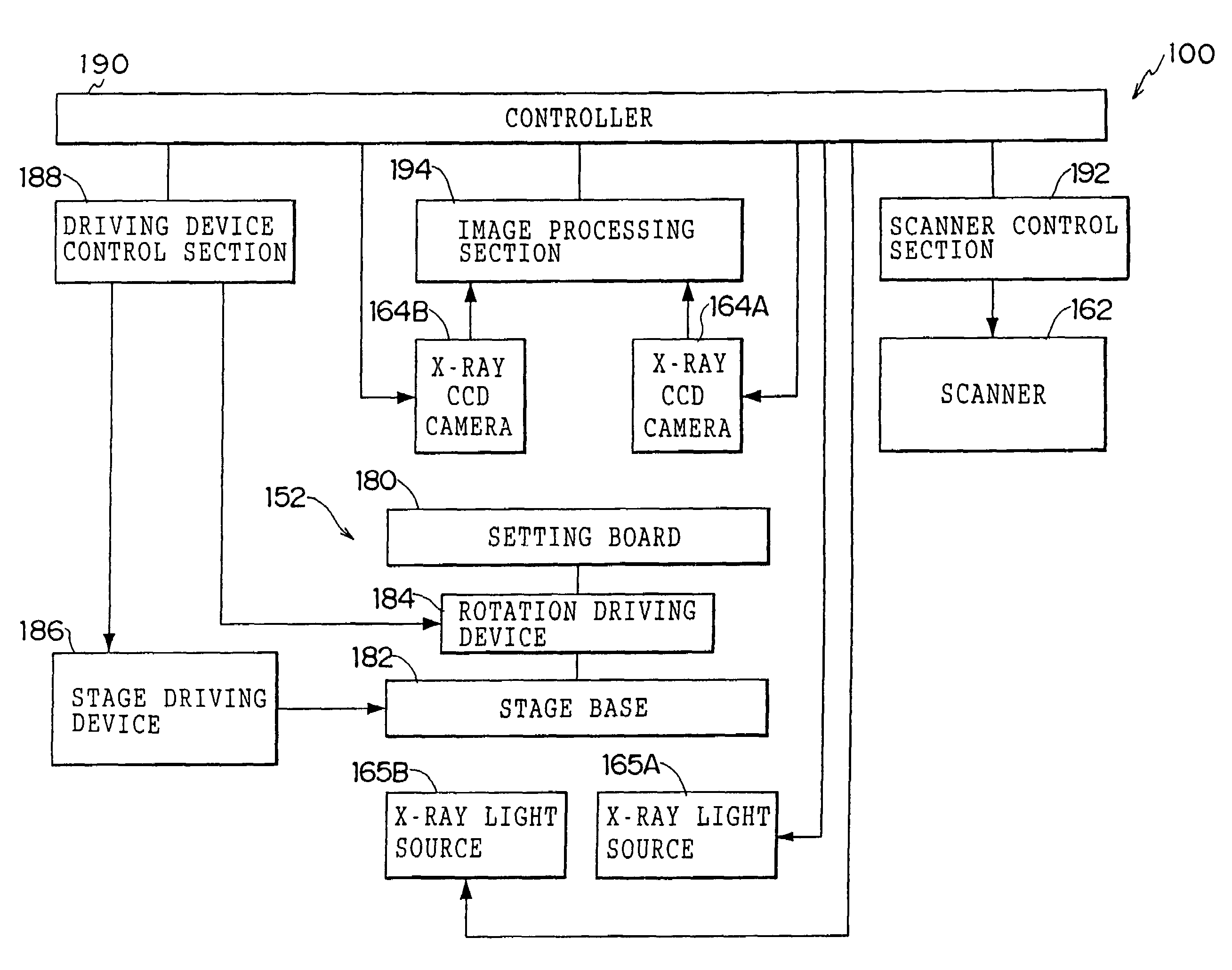
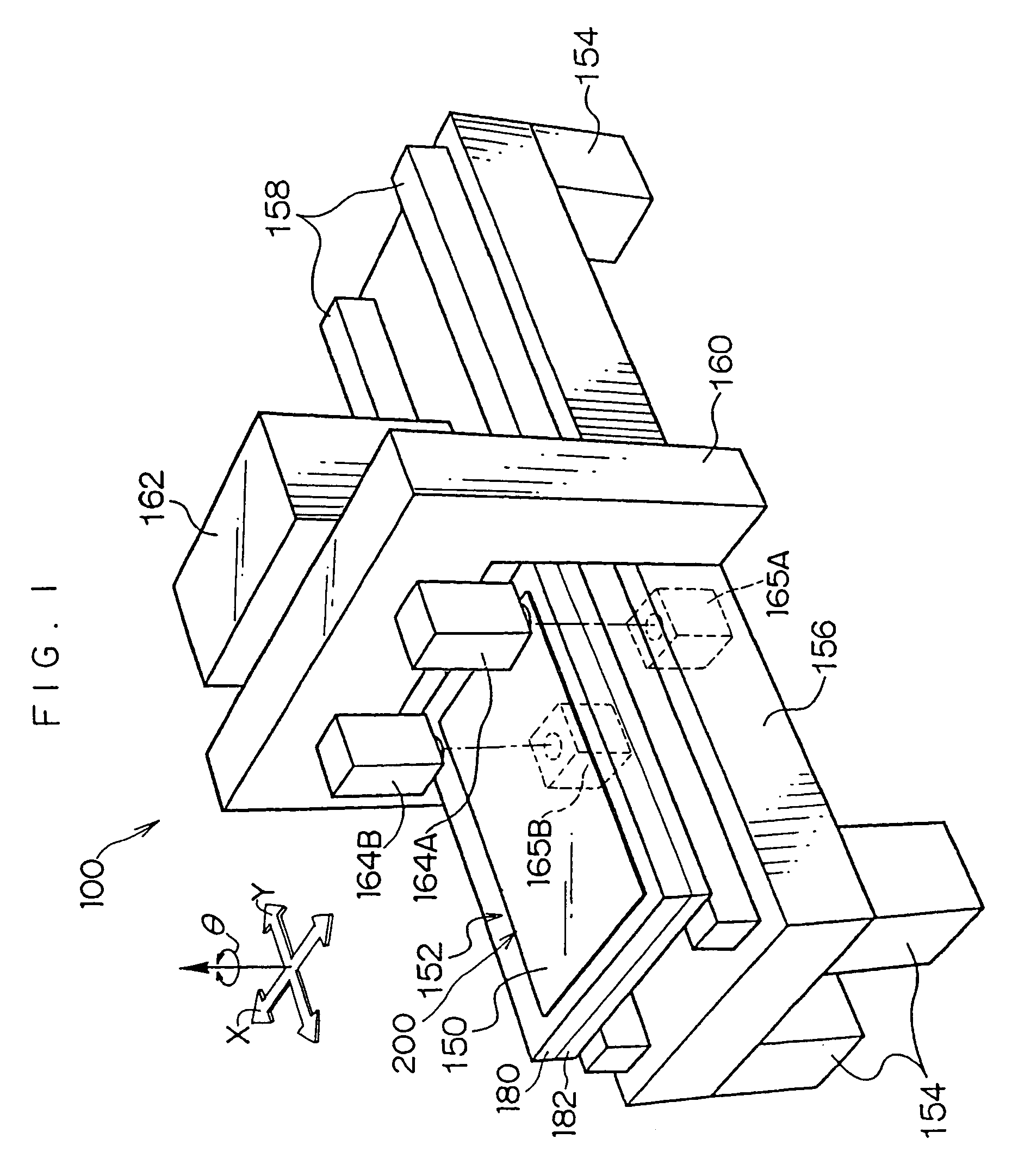
[0063]An outside view of an exposure device relating to an embodiment of the present invention is illustrated in FIG. 1 and FIG. 15 is a block diagram illustrating a schematic structure of the device.

[0064]As shown in FIG. 1, an exposure device 100 is provided with a flat plate shaped stage 152. The stage 152 holds thereon a build up wiring board material (a build up wiring board 200) on which a photosensitive material 150 is coated such that the photosensitive material 150 is absorbed on a surface of the stage 152. A thick plate shaped setting stand 156 is supported by four leg portions 154. Two guides 158 are provided in an elongating manner along stage moving directions (a direction indicated by an arrow Y in FIG. 1) on a top surface of the setting stand 156. The stage 152 is arranged such that a longitudinal direction of the stage 152 correspond...


PUM

PropertyMeasurementUnit
transmittanceaaaaaaaaaa
core diameteraaaaaaaaaa

Abstract

In order to provide an exposure device by which aligning of an exposure pattern is realized when manufacturing a build up wiring board or the like, an exposure device which exposes a photosensitive material with a light beam modulated in accordance with image information comprising a reading section which reads a radioscopic image of a specific pattern provided on an inner layer of a laminated structure, and an aligning section which aligns an exposure position of the photosensitive material laminated on a surface of an outer layer of the laminated structure on the basis of the position information of the read radioscopic image of the specific pattern, is provided.

Description

CROSS-REFERENCE TO RELATED APPLICATION[0001]This application is a continuation of U.S. patent application Ser. No. 10 / 456,680 filed on Jun. 9, 2003, now U.S. Pat. No. 6,832,045.[0002]This application claims priority under 35 USC 119 from Japanese Patent Application No. 2002-167411, the disclosure of which is incorporated by reference herein.BACKGROUND OF THE INVENTION[0003]1. Field of the Invention[0004]The present invention relates to an exposure device, and in particular, to an exposure device which exposes a photosensitive material with a light beam modulated by a space modulation element or the like in accordance with image information.[0005]2. Description of the Related Art[0006]Conventionally, various types of exposure devices, in which exposing is carried out with a light beam modulated by using a space modulation element such as a digital micro-mirror device (DMD) or the like in accordance with image data (image information), are proposed.[0007]For example, the DMD is a mirr...

Claims


Application Information

Patent Timeline
Patent Type & Authority Patents(United States)
IPC IPC(8): G03B41/00G03F7/20G03F9/00H05K1/02H05K3/00H05K3/46
CPCG03F7/70275G03F7/70291G03F9/7065G03F9/7084H05K3/4679H05K1/0269H05K2203/166H05K3/0082H05K3/4644H05K2201/09918H05K3/0008
Inventor NAKAYA, DAISUKEFUJII, TAKESHIKUDOH, YOSHIMITSU
Owner ADTEC ENG
Why Eureka
Try Eureka