
Level shifter utilizing input controlled zero threshold blocking transistors

a level shifter and zero-threshold technology, applied in logic circuits, pulse techniques, instruments, etc., can solve the problems of reducing the core supply voltage (vddb>1/b>) used in ultra-deep submicron cmos technologies, reducing driving capability, and not providing reliable operation

Active Publication Date: 2006-05-30
SAMSUNG ELECTRONICS CO LTD
View PDF5 Cites 26 Cited by
  • Summary
  • Abstract
  • Description
  • Claims
  • Application Information

AI Technical Summary

Problems solved by technology

A further difficulty in providing level shifter circuits is that the core supply voltage (vdd1) used in, for example, ultra deep submicron CMOS technologies, is reduced, while the I / O section supply voltage (vdd2) is kept at a high level.
Thus, the driving capability may be reduced to a point where the level shifter does not provide reliable operation.
For example, as the core voltage (vdd1) decreases and the difference of vdd1 and threshold voltage (Vthn) of the NMOS transistors is lowered to nearly zero, the level shifter may not provide reliable operation.
However, to reduce the threshold voltage, the transistors typically utilize thin oxides and shallow implants.
Such a thin oxide transistor may be more susceptible to voltage stress when operated in conjunction with the higher voltage vdd2.

Method used


Image

  • Level shifter utilizing input controlled zero threshold blocking transistors
  • Level shifter utilizing input controlled zero threshold blocking transistors
  • Level shifter utilizing input controlled zero threshold blocking transistors

Examples


Embodiment Construction

[0036]The present invention will now be described more fully with reference to the accompanying drawings, in which embodiments of the invention are shown. This invention may, however, be embodied in different forms and should not be construed as being limited to the embodiments set forth herein. Rather, these embodiments are provided so that this disclosure will be thorough and complete, and will fully convey the scope of the invention to those skilled in the art. Like numbers refer to like elements. As used herein the term “and / or” includes any and all combinations of one or more of the associated listed items.

[0037]It will be understood that although the terms first and second may be used herein to describe various elements, components, regions, layers, and / or sections, these elements, components, regions, layers, and / or sections should not be limited by these terms. These terms are only used to distinguish one element, component, region, layer, or section from another element, co...


PUM


Abstract

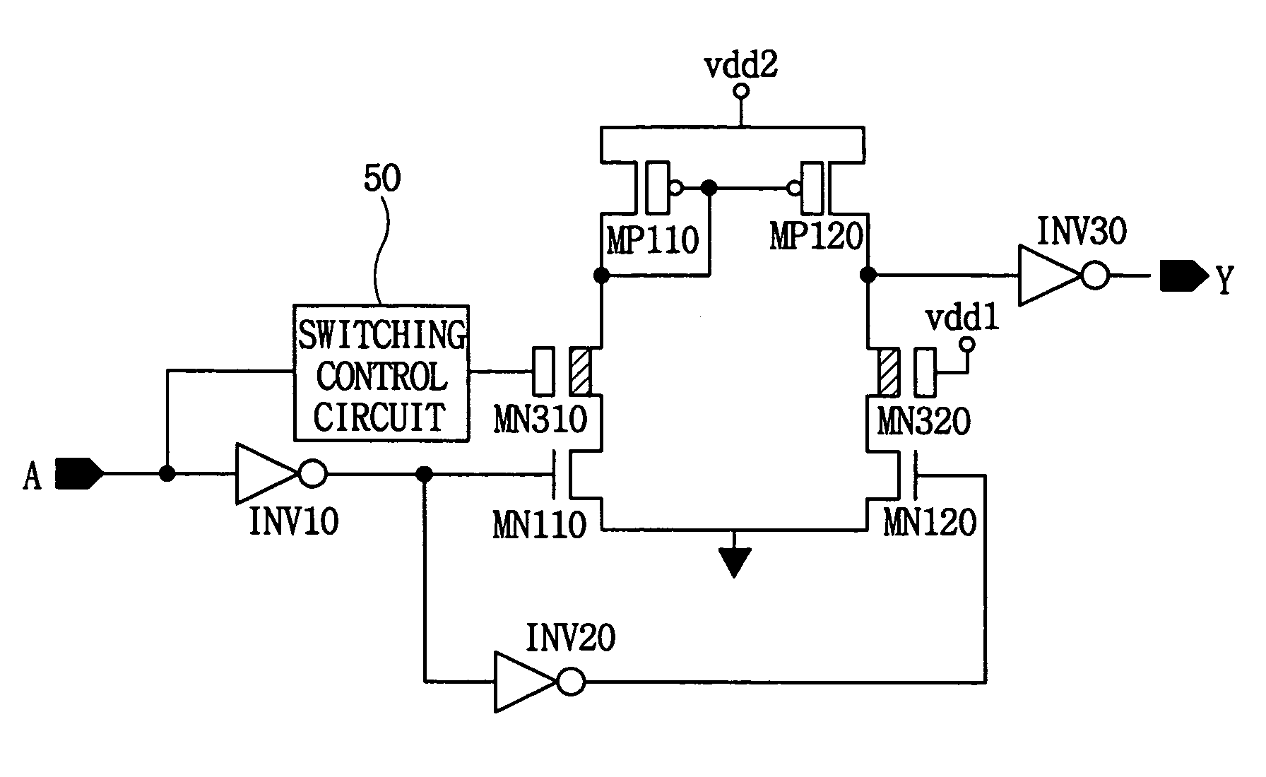
Level shifter circuits include zero threshold transistors that reduce a voltage seen by a switching transistor of the level shifter circuits and may increase blocking of static current in the level shifter circuit. The zero threshold transistors are controlled based on the input to the level shifter circuit. Thin oxide transistors may be used to provide low threshold voltages for the switching transistors. Additional level shifter circuits include serially connected zero threshold transistors that act as switching transistors in a current mirror or latch-type level shifter circuit.

Description

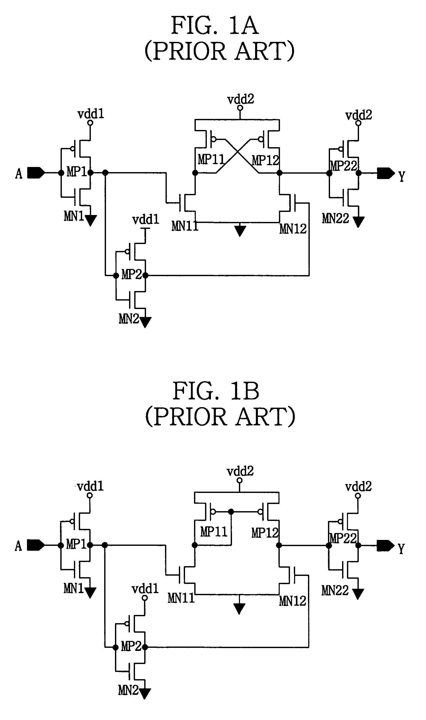
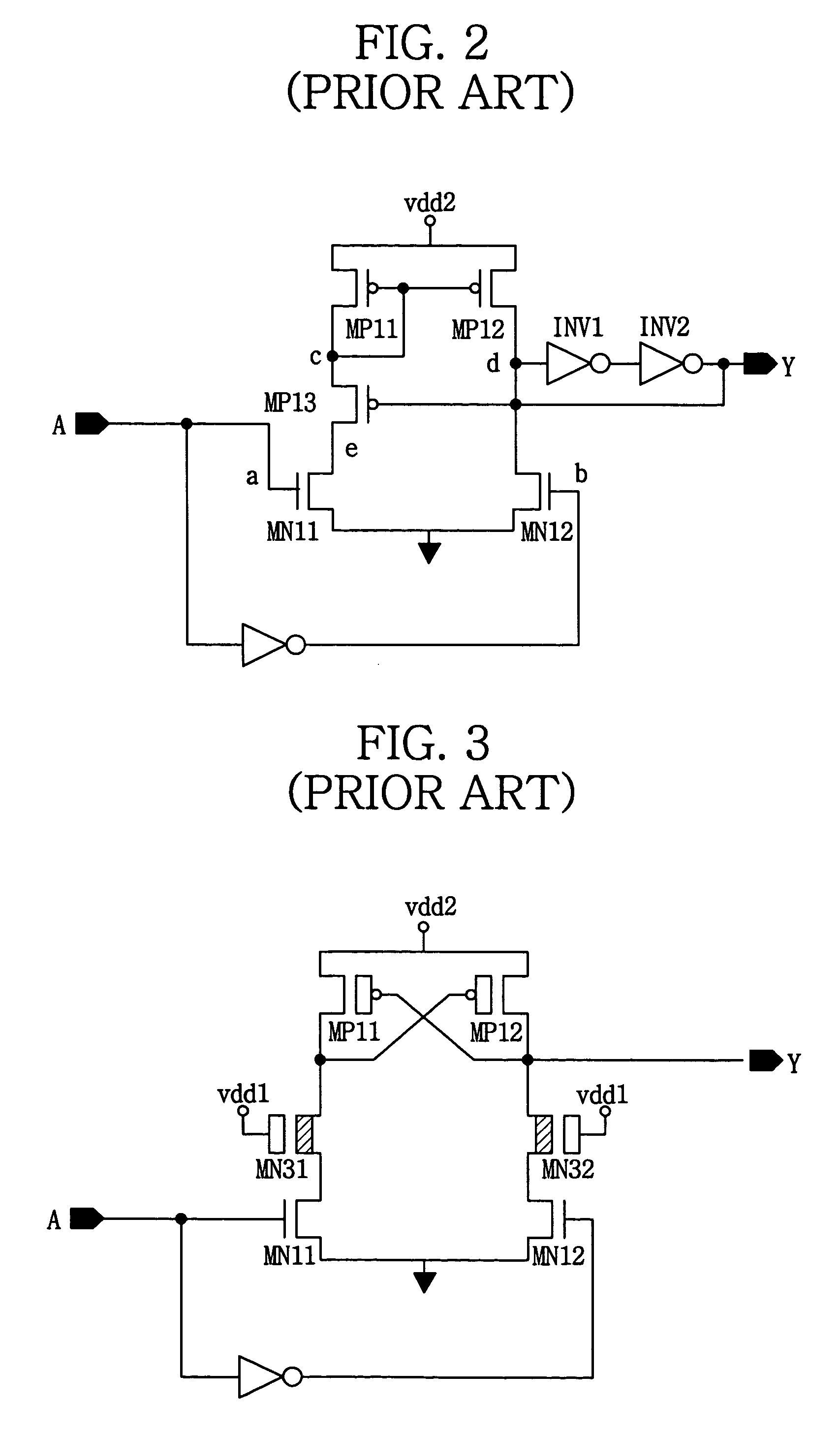
CLAIM OF PRIORITY[0001]This application claims priority from Korean Patent Application No. 10-2003-009223 1, filed on Dec. 17, 2003, in the Korean Intellectual Property Office, the contents of which are hereby incorporated by reference in their entirety as if set forth fully herein.FIELD OF THE INVENTION[0002]The present invention relates to level shifters and, more particularly, to level shifters capable of operating with technology having a very low core voltage.BACKGROUND OF THE INVENTION[0003]When connecting circuits having different power source voltages, the level of an output signal of one circuit should be shifted to the level of the other circuit receiving the output signal. In general, a level shifter accomplishes this task. As seen in FIGS. 1A and 1B, a conventional level shifter typically includes inverters and four transistors MN11, MN12, MP11, and MP12. The transistors MP11 and MP12 are p-channel MOS (PMOS) transistors, and the transistors MN11 and MN12 are n-channel M...

Claims


Application Information

Patent Timeline
Patent Type & Authority Patents(United States)
IPC IPC(8): H03K19/0175H03K19/094H03K19/0185H03K19/0948
CPCH03K19/09485H03K19/018528H03K19/0175
Inventor SEO, JIN-HO
Owner SAMSUNG ELECTRONICS CO LTD
Learn More