Self-aligned patterning method by using non-conformal film and etch back for flash memory and other semiconductor applications

a non-conformal film and patterning technology, applied in semiconductor devices, electrical equipment, transistors, etc., can solve the problems of limiting the number of memory cells, affecting the alignment of the patterning method, and affecting the alignment of the patterning process

Active Publication Date: 2008-07-17
MONTEREY RES LLC
View PDF9 Cites 28 Cited by
  • Summary
  • Abstract
  • Description
  • Claims
  • Application Information

AI Technical Summary

Problems solved by technology

Although masking techniques properly align the cells, scaling becomes an issue.
It becomes harder to place the cells closer together.
This limits how clos

Method used


Image

  • Self-aligned patterning method by using non-conformal film and etch back for flash memory and other semiconductor applications
  • Self-aligned patterning method by using non-conformal film and etch back for flash memory and other semiconductor applications
  • Self-aligned patterning method by using non-conformal film and etch back for flash memory and other semiconductor applications

Examples


Embodiment Construction

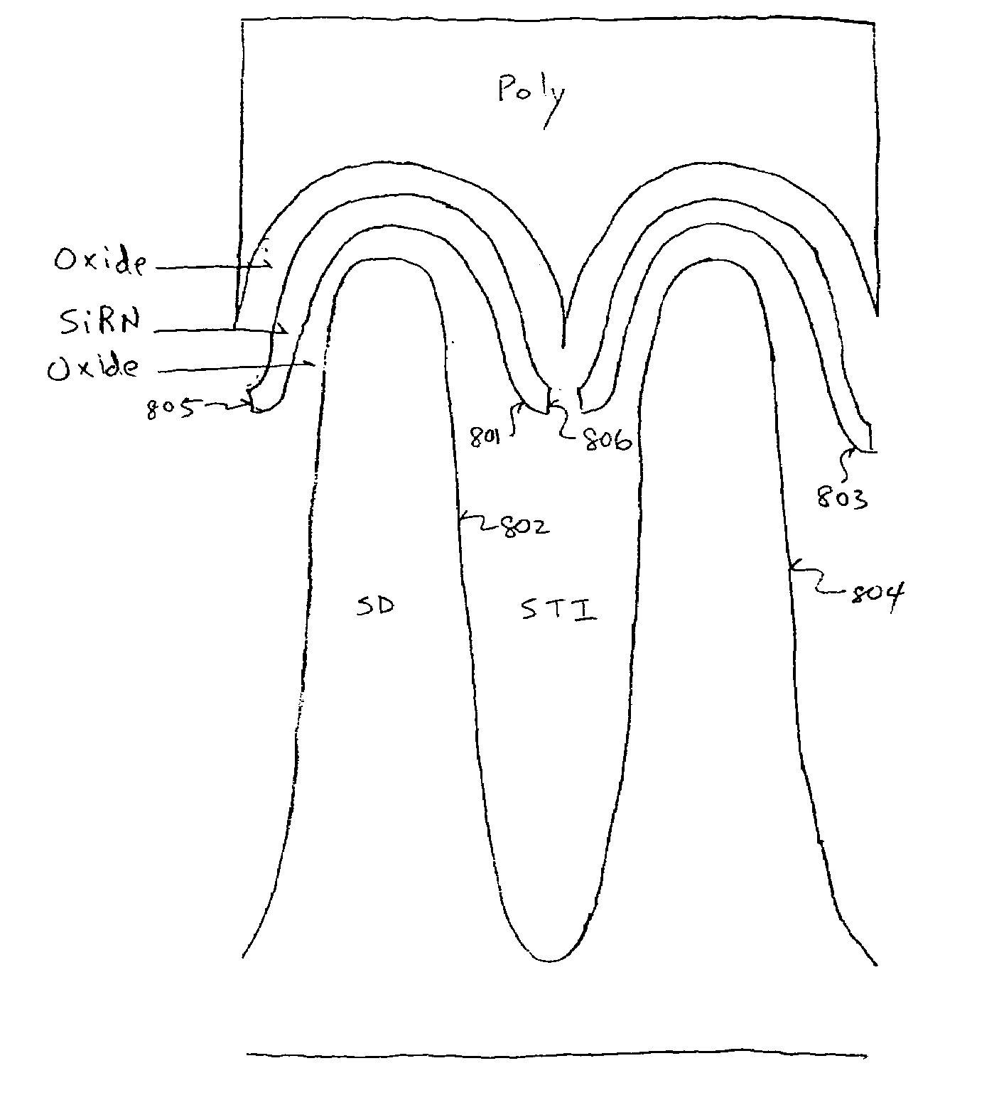
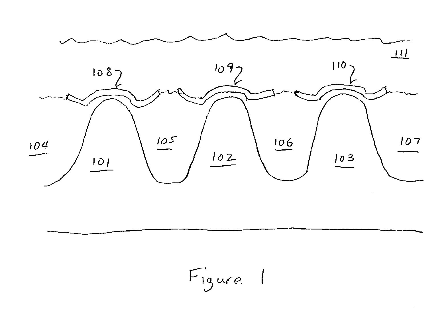
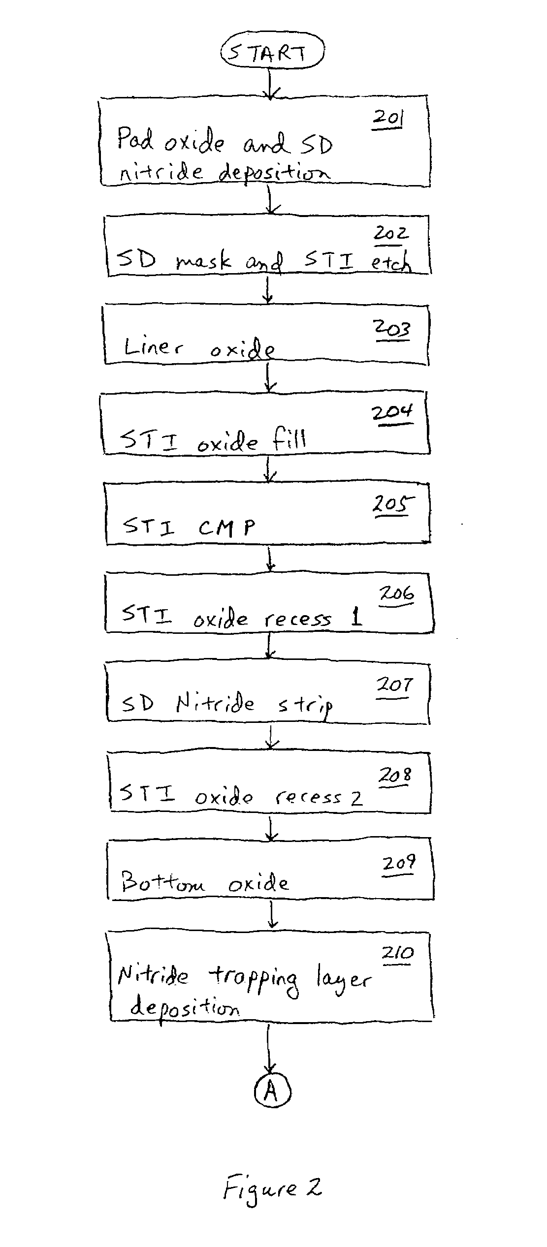
[0020]The following embodiments are described in sufficient detail to enable those skilled in the art to make and use the invention, and it is to be understood that other embodiments would be evident based on the present disclosure and that process or mechanical changes may be made without departing from the scope of the present invention. In the following description, numerous specific details are given to provide a thorough understanding of the invention. However, it will be apparent that the invention may be practiced without these specific details. In order to avoid obscuring the present invention, some well-known system configurations and process steps are not disclosed in detail. Likewise, the drawings showing embodiments of the invention are semi-diagrammatic and not drawn to scale, and particularly, some of the dimensions are for the clarity of presentation and are shown exaggerated in the Figures.

[0021]Generally, the present invention provides a method for manufacturing a s...


PUM


Abstract

A method for fabricating a memory device with a self-aligned trap layer which is optimized for scaling is disclosed. In the present invention, a non-conformal oxide is deposited over the charge trapping layer to form a thick oxide on top of the core source/drain region and a pinch off and a void at the top of the STI trench. An etch is performed on the pinch-off oxide and the thin oxide on the trapping layer on the STI oxide. The trapping layer is then partially etched between the core cells. A dip-off of the oxide on the trapping layer is performed. And a top oxide is formed. The top oxide converts the remaining trap layer to oxide and thus isolate the trap layer.

Description

FIELD OF THE INVENTION[0001]The present invention relates, in general, to a self-aligned process for fabricating semiconductor memory devices by using a non-conformal film and etch back process.BACKGROUND OF THE INVENTION[0002]Data is digitally stored in semiconductor memory devices. These semiconductor memory devices fall into one of two categories. Volatile memory devices retain their data only when they are powered on; whereas, non-volatile memory chips can retain the data even if no external power is being supplied to the memory device. One popular form of non-volatile memory device is flash memory. Flash memory is versatile because it can be erased and programmed multiple times. Furthermore, flash memory is relatively inexpensive compared to other types of non-volatile memory devices. Consequently, flash memory is ideal for applications that demand significant amounts of non-volatile, solid-state storage. Examples of applications employing flash memory include USB flash drives,...

Claims


Application Information

Patent Timeline
IPC IPC(8): H01L21/336
CPCH01L27/11568H01L27/115H10B43/30H10B69/00
Inventor FANG, SHENGINGCHANG, KUO-TUNGTHURGATE, TIMSUH, YOUSEOKHOLBROOK, ALLISON
Owner MONTEREY RES LLC
Why Eureka
Try Eureka