High-voltage ESD (electro-static discharge) protective device triggered by bidirectional substrate

An ESD protection, high-voltage technology, applied in the direction of electric solid devices, semiconductor devices, electrical components, etc., to achieve the effect of reducing on-resistance, strong current discharge ability, and expanding the scope of application

Active Publication Date: 2013-03-13
铜陵汇泽科技信息咨询有限公司
View PDF8 Cites 25 Cited by
  • Summary
  • Abstract
  • Description
  • Claims
  • Application Information

AI Technical Summary

Problems solved by technology

The present invention provides a new technical solution, and designs a high-voltage ESD protection device with strong anti-latch ability and strong robustness, which can greatly reduce the risk of circuit function failure caused by ESD.

Method used


Image

  • High-voltage ESD (electro-static discharge) protective device triggered by bidirectional substrate
  • High-voltage ESD (electro-static discharge) protective device triggered by bidirectional substrate
  • High-voltage ESD (electro-static discharge) protective device triggered by bidirectional substrate

Examples


Embodiment Construction

[0026] The present invention will be described in further detail below in conjunction with the accompanying drawings and specific embodiments:

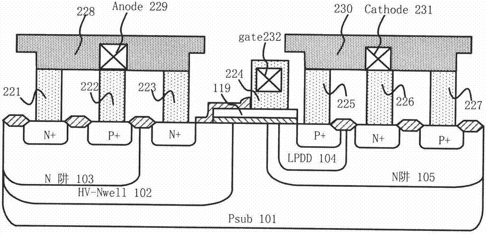
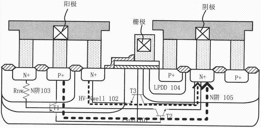
[0027] The present invention proposes a bidirectional substrate-triggered high-voltage ESD protection device. Due to the special design of the internal structure and the optimization of the layout level, the example device of the present invention has the SCR structure ESD protection device with fast turn-on speed, low on-resistance, and low on-resistance. The advantage of large secondary breakdown current and its internal parasitic NPN structure can provide high maintenance voltage for LDMOS devices, which further increases the robustness of the device. Expand the scope of application of the device of the present invention.

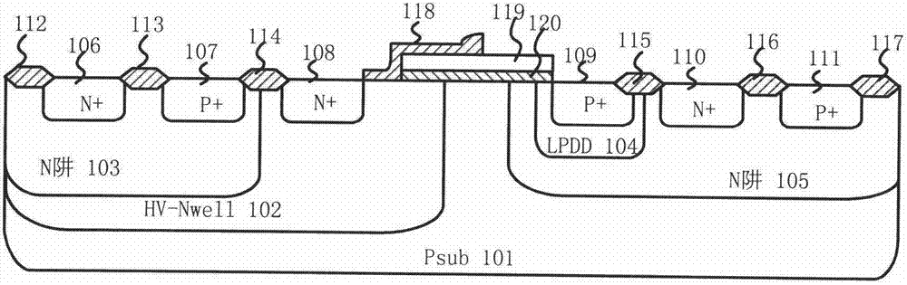
[0028] like figure 1 As shown, it is a cross-sectional view of the internal structure of the device of the present invention, which is mainly composed of a substrate Psub 101, a high-voltage deep N-well 102, a ...


PUM


Abstract

The invention discloses a high-voltage ESD (electro-static discharge) protective device triggered by a bidirectional substrate. The high-voltage ESD protective device triggered by the bidirectional substrate can be used for an on-chip IC (integrated circuit) ESD protective circuit and mainly comprises a substrate Psub, a high-voltage deep N trap, a lightly doped p-type drift region, a first highly doped N+ injection region, a first P+ injection region, a second N+ injection region, a second P+ injection region, a third N+ injection region, a third P+ injection region, a polycrystalline silicon grid, a grid thin oxide layer and a plurality of field oxide isolation regions. Reverse PN nodes at the interface part of the high-voltage N well or the N well and the substrate can be triggered and conducted through the forward and reverse ESD high-voltage pulse effect, two structures of internal SCR (silicon controlled rectifier) and LDMOS (laterally diffused metal oxide semiconductor) operate at the same time so as to form an ESD current discharge path to improve the secondary breakdown current of the device and lower the conducted resistance. The maintaining voltage of the device is improved through hoisting the channel length of the LDMOS device, the internal structure design as well as optimization of layout hierarchy, and the high-performance ESD protection is realized.

Description

technical field [0001] The invention belongs to the field of electrostatic protection of integrated circuits, and relates to a high-voltage ESD protection device, in particular to a high-voltage ESD protection device triggered by a bidirectional substrate, which can be used to improve the reliability of on-chip high-voltage ESD protection. Background technique [0002] With the rapid development of intelligent power technology and high-power semiconductor devices, electronic products are increasingly miniaturized and portable, and the application fields of power electronic devices are constantly expanding. According to the survey, among the various factors that lead to the failure of power electronic devices and their IC functions, ESD is the main factor for the failure of devices and their ICs. This is because the devices or products may generate static electricity during manufacturing, packaging, testing and use. , When people make these objects contact each other without ...

Claims


Application Information

Patent Timeline
Patent Type & Authority Applications(China)
IPC IPC(8): H01L27/02
Inventor 梁海莲顾晓峰董树荣黄龙
Owner 铜陵汇泽科技信息咨询有限公司
Why Eureka
Try Eureka