

Display device
a display device and display technology, applied in the field of electronic displays, can solve the problem of not being able to achieve desired gradation
- Summary
- Abstract
- Description
- Claims
- Application Information
AI Technical Summary
Benefits of technology
Problems solved by technology
Method used
Image

Examples
embodiment 1
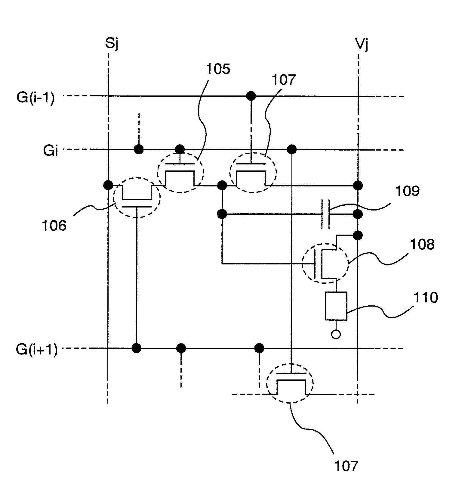
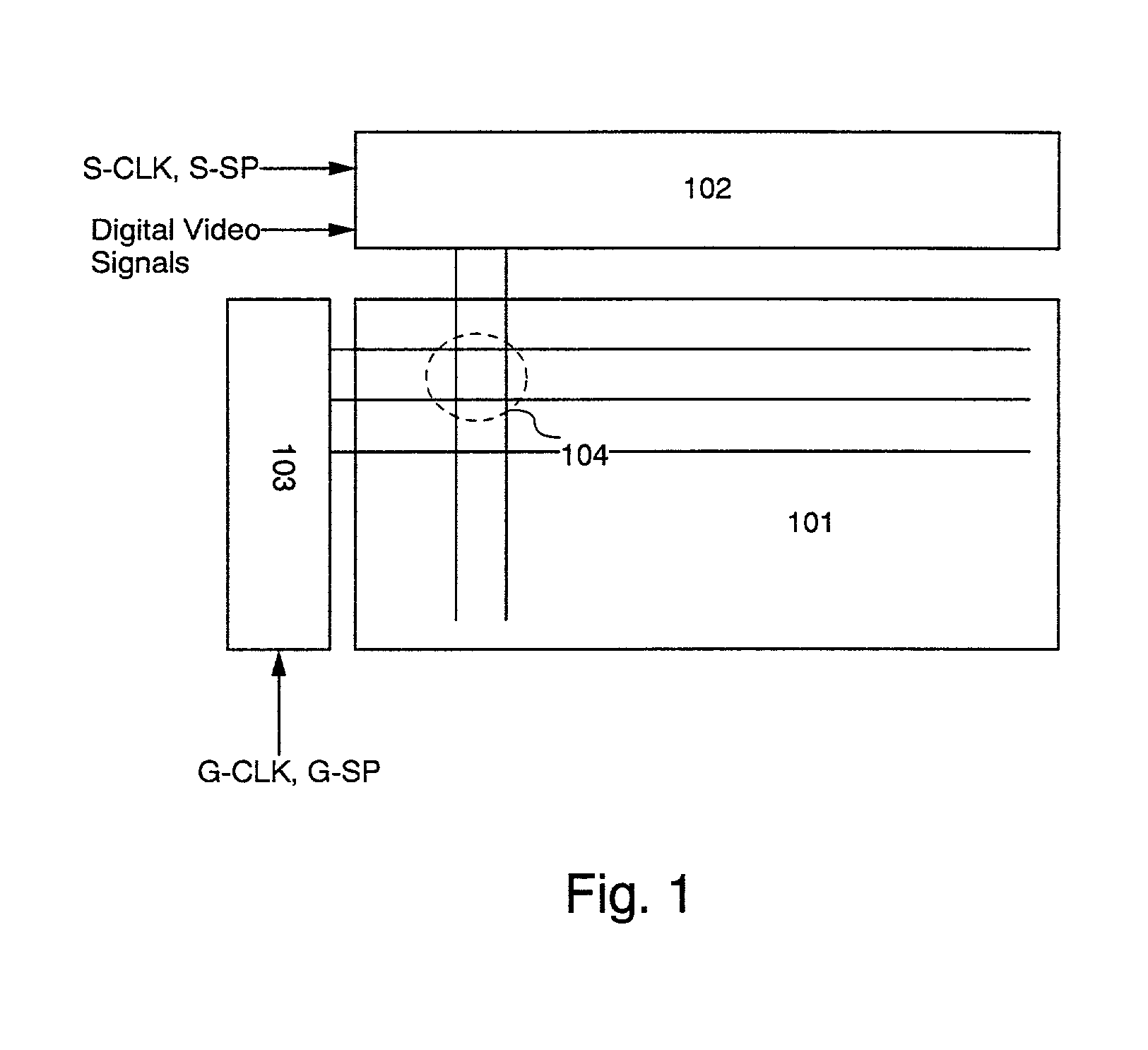
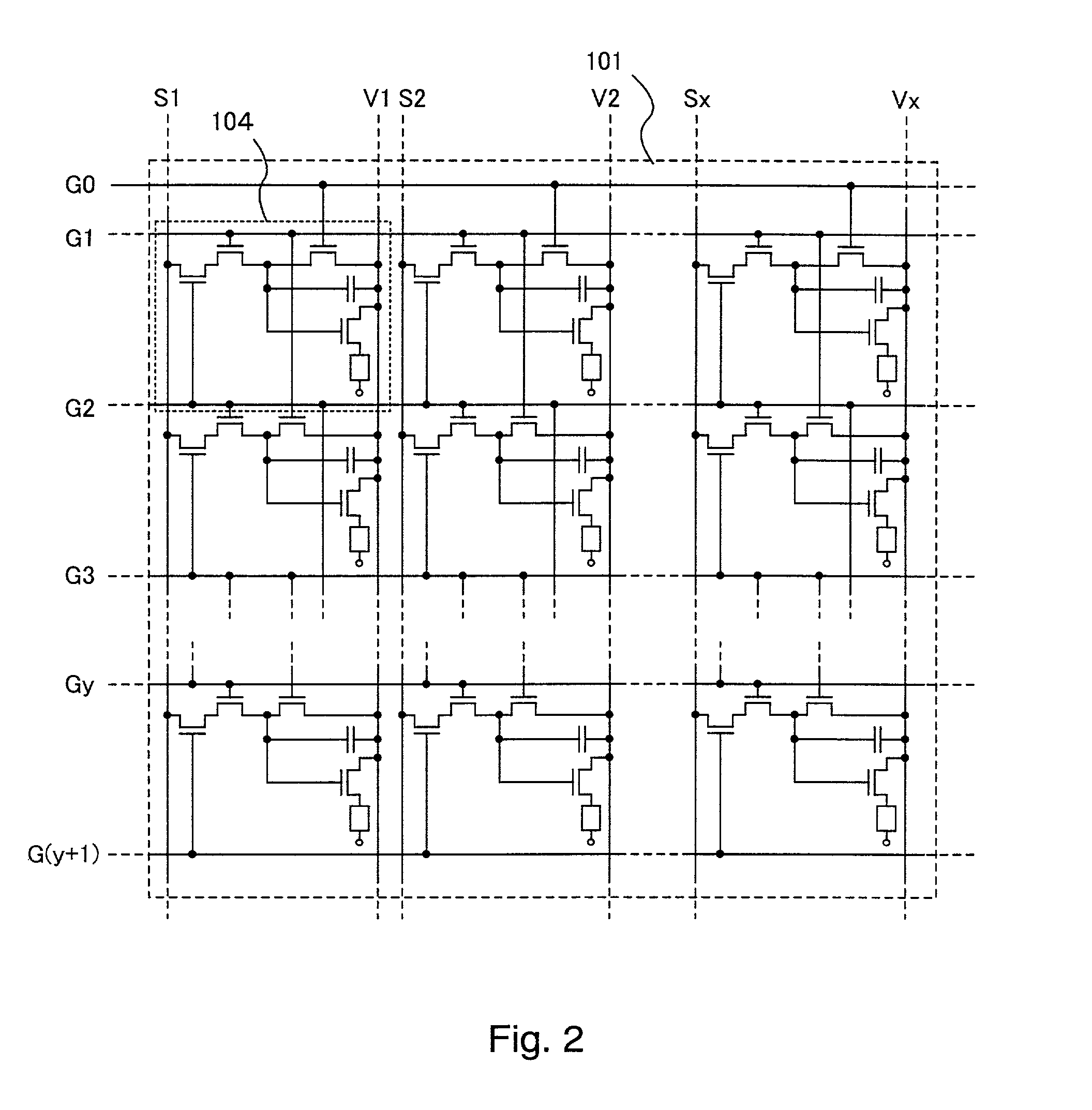
[0141]In the present embodiment, a case where 26 tones are displayed according to a 6-bit digital video signal in an EL display according to the present invention is described with reference to FIG. 6. It is to be noted that the EL display of the present embodiment has the structure illustrated in FIGS. 1 to 3.
[0142]First, during a writing period Ta1, the gate signal line G0 is selected according to a selection signal for writing inputted from the gate signal line driver circuit 103 to the gate signal line G0. Then, the TFTs 107 for erasing of the pixels in the first line whose the gate electrodes are connected to the gate signal line G0 are turned on. When the TFT 107 for erasing is turned on, the gate electrode and the source region of the TFT 108 for EL driving are electrically connected to each other. Therefore, the gate voltage (the potential difference between the gate electrode and the source region) of the TFT 108 for EL driving becomes zero, which makes the TFTs 108 for EL ...
embodiment 2
[0177]In the present example, the order of appearance of the display periods Tr1 to Tr6 is described in a driving method according to the present invention which is adapted for a 6-bit digital video signal.
[0178]FIG. 7 illustrates a timing chart of a driving method of the present example. The specific driving method is described in Embodiment 1, and thus, the description thereof is omitted here. In the driving method of the present embodiment, a longest non-display period (Td1 in the present embodiment) in one frame period is provided last in the one frame period. By this structure, human eyes visually perceive that there is a pause between the non-display period Td1 and the first display period of the next frame period (Tr4 in the present embodiment). This makes it possible to make less recognizable to human eyes display unevenness caused due to adjacent display periods of light emission of adjacent frame periods when halftone display is carried out.
[0179]It is to be noted that, th...
embodiment 3
[0180]In the present example, a case where 24 tones are displayed according to a 4-bit digital video signal in an EL display according to the present invention is described with reference to FIG. 8. It is to be noted that the EL display of the present embodiment has the structure illustrated in FIGS. 1 to 3.
[0181]First, during a writing period Ta1, the gate signal line G0 is selected according to a selection signal for writing inputted from the gate signal line driver circuit 103 to the gate signal line G0. Then, the TFTs 107 for erasing of the pixels in the first line whose gate electrodes are connected to the gate signal line G0 are turned on. When the TFT 107 for erasing is turned on, the gate electrode and the source region of the TFT 108 for EL driving are electrically connected to each other. Therefore, the gate voltage (the potential difference between the gate electrode and the source region) of the TFT 108 for EL driving becomes zero, which makes the TFTs 108 for EL driving...
PUM
 Abstract
Description
Claims
Application Information