Image sensor and fabricating method thereof

a technology of image sensor and fabricating method, which is applied in the field of optical devices, can solve the problems of low yield rate of conventional cmos image sensor b>100/b> and complicated layout design, and achieve the effect of improving yield rate and high contrast ratio

Active Publication Date: 2006-06-13
UNITED MICROELECTRONICS CORP
View PDF13 Cites 18 Cited by
  • Summary
  • Abstract
  • Description
  • Claims
  • Application Information

AI Technical Summary

Benefits of technology

[0009]The present invention provides a method of fabricating an image sensor, which has a high contrast ratio, which in turn, improves yield rate during the fabricating processes.
[0023]In the image sensor of the present invention, the sensing devices in the image sensing device layer directly receive the light passing through the SOI layer which has a small thickness. Next, an electrical signal, which represents image information received by the sensing devices, is output to a printed circuit board through bonding pads and bumps. Therefore, the degradation of the light resulting from absorption or reflection by the inter-dielectric layer and the metal layer of the interconnection layer does not occur, and thereby the sensitivity of the sensing devices is improved significantly. Furthermore, the complexity of the fabrication process is lowered as layout of conductive layers can be distributed over the entire area of the image sensing device layer.

Problems solved by technology

However, this makes the layout design complicated.
Furthermore, the yield rate of the conventional CMOS image sensor 100 is also low.

Method used


Image

  • Image sensor and fabricating method thereof
  • Image sensor and fabricating method thereof
  • Image sensor and fabricating method thereof

Examples


Embodiment Construction

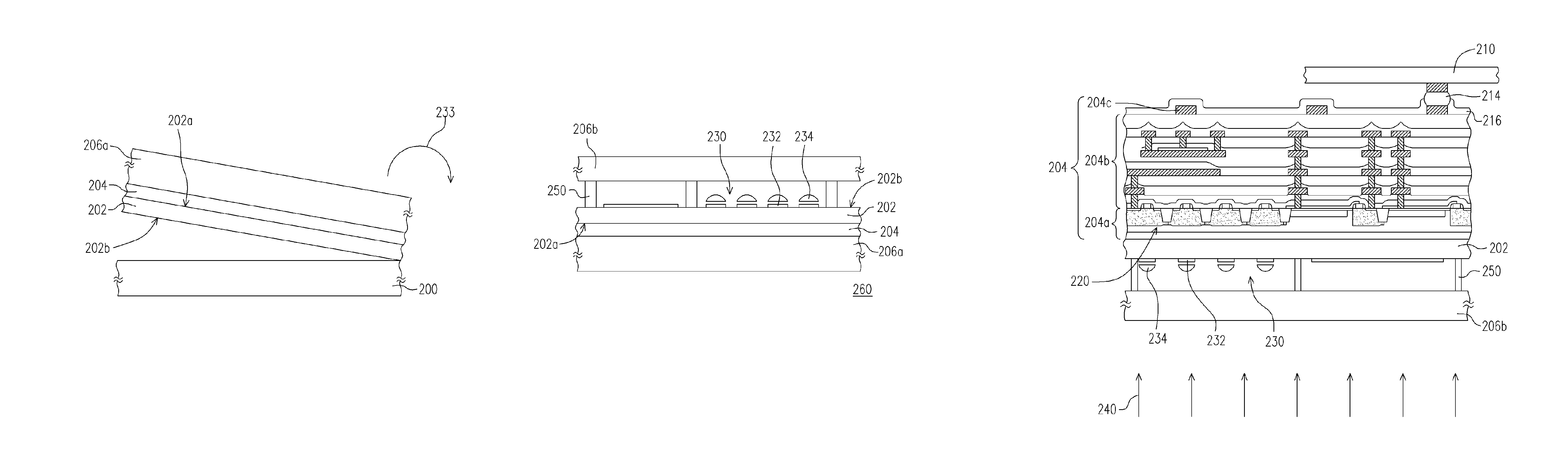
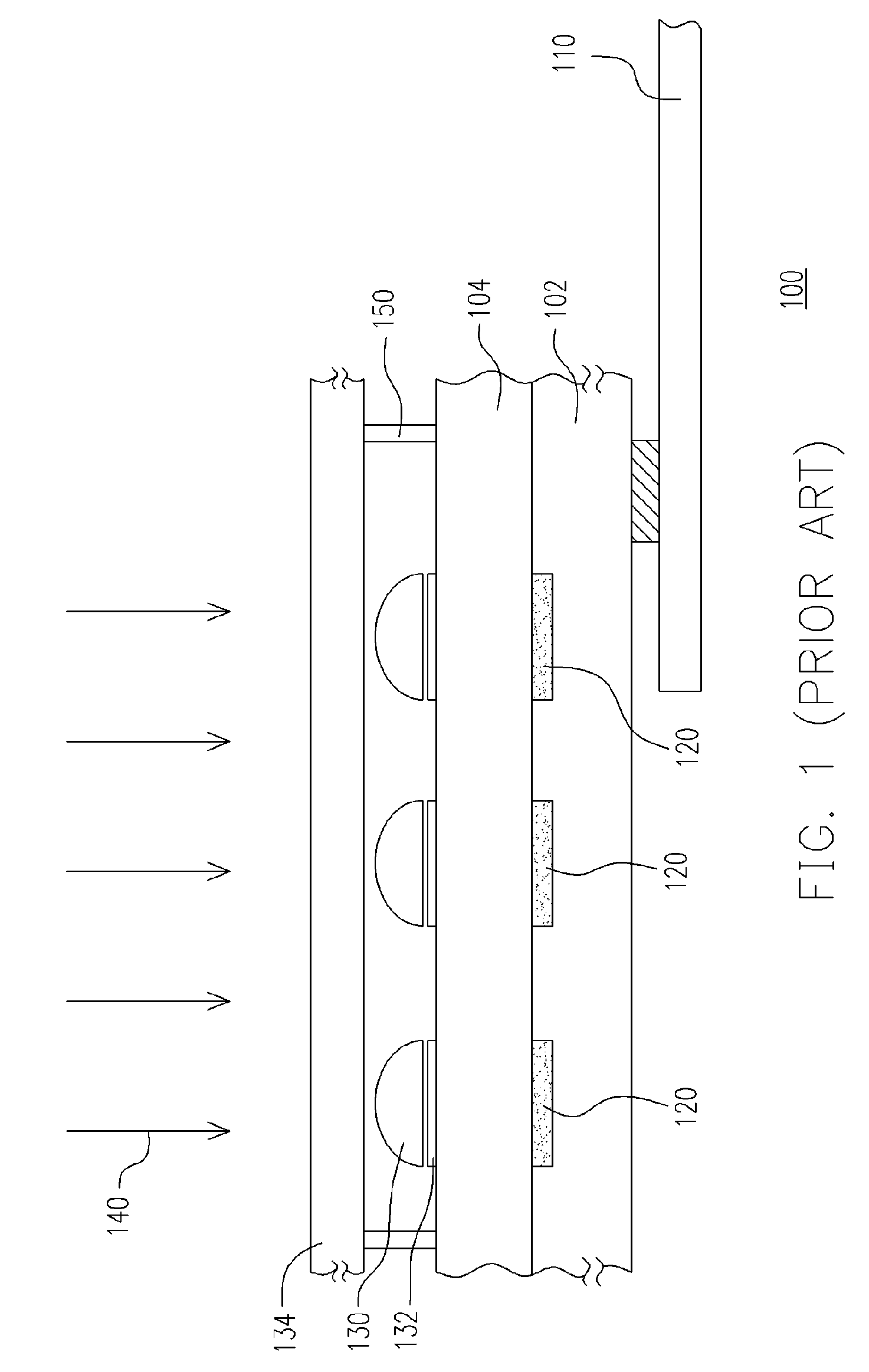
[0029]The image sensor of the present invention, which has a short path over which incident light passes, is fabricated using a process, which enhances the optical performance of the image sensor. A CMOS image sensor is merely an example used for explaining the design and working of the present invention. Applications of the present invention are not limited to CMOS image sensors.

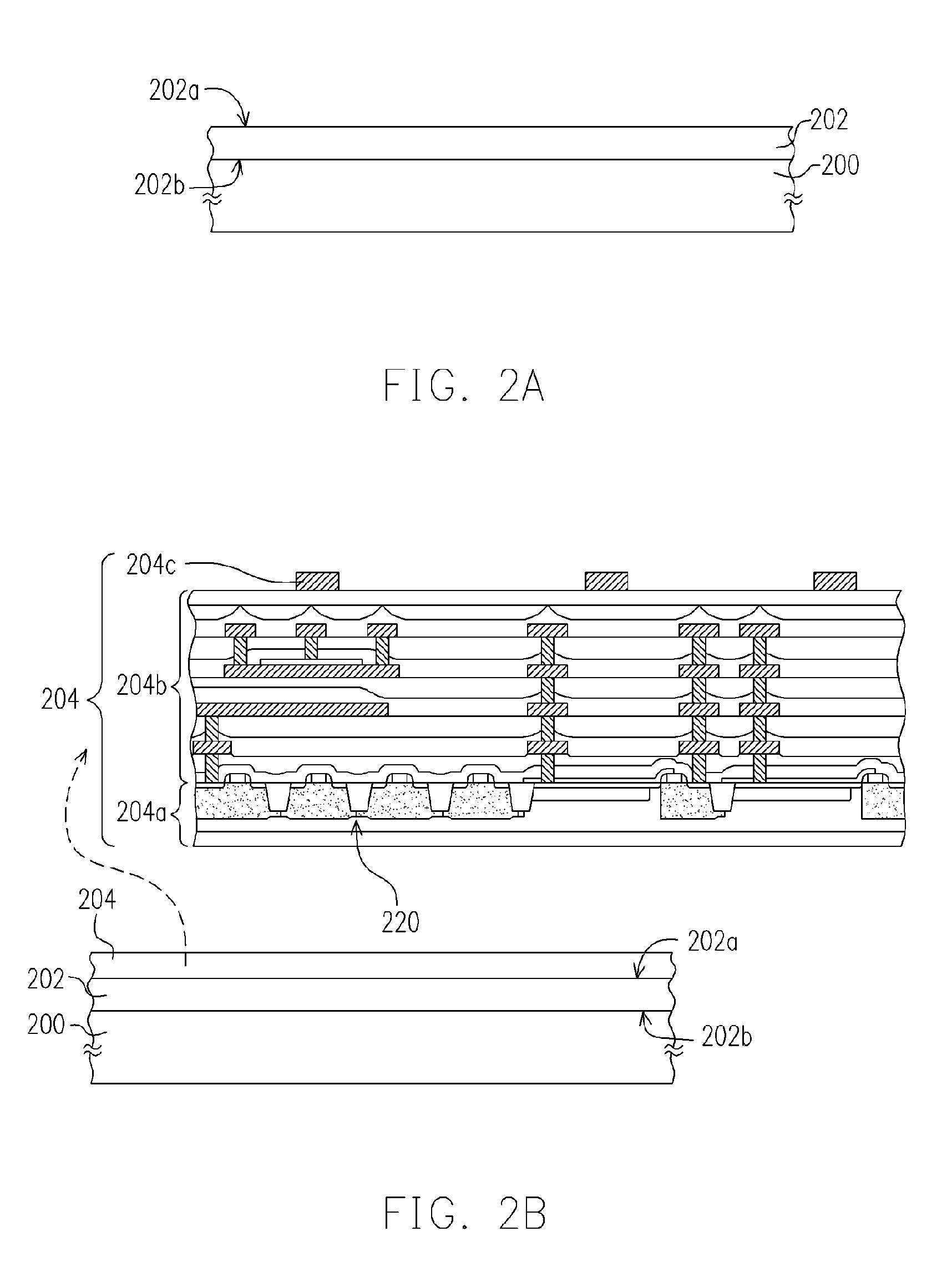
[0030]FIG. 2A to FIG. 2E are schematic illustrations of the fabricating process of a CMOS image sensor in accordance with an embodiment of the present invention. Referring to FIG. 2A, first, a silicon on insulator layer (SOI layer) 202, which has a first surface 202a and a second surface 202b is formed over a substrate 200. The substrate 200 is, for example, a silicon wafer. In accordance with an embodiment of the present invention, the fabricating process of the SOI layer 202 is a conventional process, which is well known by persons skilled in the art. Therefore, details of the fabricating process are not ...


PUM


Abstract

An image sensor comprising an image sensing device layer, a silicon-on-insulator (SOI) layer, an optical device array and a substrate is provided. The SOI layer has a first surface and a second surface. The image sensing device layer is formed on the first surface of the SOI layer. The optical device array is formed on the second surface of the SOI layer. The substrate is disposed above the second surface of the SOI layer and the optical device array is disposed between the substrate and the SOI layer. An incident light coming from the outside environment, passes through the optical device array and the SOI layer, and is received by sensing devices formed in the image sensing device layer. In this manner, the probability of absorption or reflection of the incident light is reduced. Therefore, the sensing performance and the yield of the image sensor of the present invention is improved.

Description

BACKGROUND OF THE INVENTION[0001]1. Field of Invention[0002]The present invention relates to an optical device and a fabricating method thereof. More specifically, the present invention relates to an image sensor and a fabricating method thereof.[0003]2. Description of Related Art[0004]With the popularization of multimedia, various digital image devices have been developed sequentially. An image sensor being a key component of digital image devices has gained significant importance. The function of an image sensor is to transform image information into electrical signals. Image sensors may be categorized into various types, such as charge coupled device image sensors (CCD image sensor), complementary metal oxide semiconductor image sensors (CMOS image sensor) etc. Due to low cost, low power consumption, random access ability and high integration ability, CMOS image sensors are widely used in popular products, such as camera phone and web-cameras.[0005]FIG. 1 illustrates a schematic ...

Claims


Application Information

Patent Timeline
Patent Type & Authority Patents(United States)
IPC IPC(8): H01L21/30H01L21/46
CPCH01L27/14618H01L27/14621H01L27/1464H01L27/14636H01L27/14685H01L27/14627H01L2924/0002H01L2924/00
Inventor PAN, JUI-HSIANGSUN, CHENG-KUANGCHENG, KUANG-CHIHLEE, KUANG-SHIN
Owner UNITED MICROELECTRONICS CORP
Why Eureka
Try Eureka